Using Nullors to Modify Linear Model Parameters of Transistors in an Analog Circuit

Adv. Sci. Technol. Eng. Syst. J. 3(5), 439–446 (2018);
 DOI: 10.25046/aj030550
Usually, after properly biasing an analog circuit we need to linearize its transistors in order to linearize the entire circuit for performance analysis and design. This linearization is done through modeling of devices, which is becoming more and more complicated as the electronic technology advances. This is not of course a major issue for circuit simulators that use the latest device models and fast computers to deal with them. However, it makes it difficult when manual computation and understanding of the circuit behavior is in question. This is particularly important in teaching and training electrical engineering students. What the proposed method offers is to simplify the case in two steps. First, adopt a most recent model with nominal parameter values for the transistors and run the circuit. Second, compare the circuit responses with those obtained through simulators with the most advanced device models. Next, with the help of one or more nullors try to modify the manually selected model parameters so that the two responses become close enough together. Several examples demonstrate the way the technique works and how close we can get to the simulated responses.
1. Introduction
Linearizing analog circuits is a major step in circuit analysis and simulation, preparing for performance analysis and design. However, it is also important to understand the circuit behavior for design purposes. This is particularly essential in teaching students/designers in the field of electrical engineering. With so fast changing electronic technology and the transistors’ modeling techniques, this linearization process becomes very cumbersome when it comes to hand calculations and manual circuit verifications and evaluations [1-3].
Several strategies can be proposed. A simple and effective one is to apply external probing such as experimenting with the transistors in different circuits and study their behavior, and then start building a working model. Alternatively, we can manually linearize the transistors to our best knowledge, and with an available and appropriate model that we think is working. Then we can compare responses from this circuit with those we get from an advances circuit simulator. This definitely will guide us to modify our model for a better accuracy. Here, in this study we are trying to focus on this proposed methodology. It is interesting to note that the proposed technique takes a full advantage of the computational power and the precision expected from a modern circuit simulator, in order to direct the manually modeling procedure to achieve its goals.
Here is how the method works. Let us first assume a circuit that has only one transistor. We choose a linear small signal equivalent circuit model for the transistor in the circuit that best represents the device modeling. This apparently linearizes the entire circuit and prepares it for the AC analysis. Our next step is to simulate the circuit. However, to be certain about the direction we take for the modification of the model elements, this simulation is done in combination with the circuit with the original transistor. The combined circuits here are connected in parallel-parallel format. Other formats are also possible, such as series-series, parallel-series, and series-parallel, depending on the types of the input and output ports. In this connection both circuits get the same input signal and will produce identical outputs. Naturally, considering circuit laws, this identical outputs cannot happen unless we allow an extra degree of freedom in the linearized circuit. To fulfill this task one component in the linearized model is allowed to freely change its variables (v and i) values, which basically becomes a norator. The final step is to find a closest real component (or any two-terminal circuit) that best suits to replace the norator.
In short, there are two main steps involved here. In the first step the analog circuit is manually linearized after the biasing is completed and the regions of the operations for the transistors are specified. This will allow us to roughly assign linearized model parameters to the devices and hence make the entire circuit linear. In the second step this linear circuit is linked to the actual nonlinear circuit, in its original form, and the combined circuit is simulated with the constraint that both circuits produce the same responses, without interfering each other’s operations. This process can of course be repeated for as many times as needed, depending on the precision required. In each process a different model component is selected for change, or alternatively, new components can be added to the model until we are satisfied.
Overall, using this procedure gets us closer and closer to the ideal response for the application we have. In exchange the price we need to pay is to modify one or more device model components in a manner in which the output response will improve to the ideal case even when we disconnect the two circuits from each other. This means, the linear circuit responds favorably after being separated from the original circuit. It must also be noted that this similarity in responses must only be valid for a certain region of operation, and for a desired bandwidth. That is, depending on the selections of the model components, the situation only needs to work for the application in hand and the frequency bandwidth described. Outside of this region of operation or bandwidth the response may or may not match with that of the original circuit.
The crucial components that are used for such operations are nullors, which are special types of fixator-norator pairs (FNP) [4-10]. Nullors are among pathological elements that although not ideally available in physical form but have very unique properties particularly for circuit designs [8, 9]. Briefly, a nullor consists of a pair of elements, a nullator and a norator. A nullator element passes zero current and has zero voltage across, whereas, a norator element has both its current and voltage unspecified. The difference between a nullor and an FNP is in the nullator element. In case the nullator in a nullor allows to have any arbitrary (but fixed) current or voltage then the nullor becomes an FNP. When used in pairs the nullator keeps both component variables (v and i) fixed, whereas both variables of the pairing norator are specified by the circuit. It is this unique property that makes a nullor well suited for design purposes. And here we exactly use the pair to adjust and modify the transistor model parameters in order to make the linearized circuit to perform as specified.
Finally, it must be pointed out that there is no claim this methodology can replace a formal and accurate transistor modeling, which is typically used by circuit simulators. The main purpose of using this technique is to educate electrical engineering students to manually experiment with device modeling for different applications. In addition, the approach simplifies and makes it more understandable to study circuit behavior such as finding poles and zeros and frequency behavior of the circuit. Although not still to its perfection, the method seems to be new and practical. As far as this author is aware of, there is no similar method reported in the literature to compare.
2. Modification of Model Parameters in a Linearized Circuit
The objective in this presentation is to linearize an analog circuit with transistors after being biased for a certain application. This is needed to perform further analysis such as AC analysis, transient analysis, and also for performance design [11]. A typical performance design procedure for amplifiers and analog filters is to design for frequency profile and bandwidth. To do this we need to first linearize the devices in the circuit and come up with a linear circuit. The next step is to perform AC analysis on the circuit using a circuit simulator. The procedure is done by first replacing the transistors in the circuit with their small signal linear models that are constructed from the device characterization and parameters extractions. Depending on several factors, such as the fabrication technology used, device sizes, and the transistors’ modeling levels (in Spice) being adopted, these model parameters can become very complicated for manual considerations. They may even change whether we use them for analog design or digital. In general getting quite accurate model parameters mainly for short channel MOS transistors, for example, is not a trivial task. Figures 1 and 2 are examples of simpler linearized models for longer channel lengths MOS transistors.
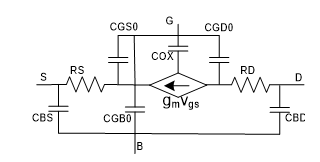 Figure 1. SPICE Level 1 Model for long channel MOS transistors.
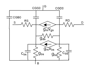 Figure2. SPICE Level 3 Model for long channel MOS transistors.
Figures 1 is the Level 1 model for long channel MOS transistors adopted by SPICE simulation program, and Fig. 2 is the schematic of a more advanced, Level 3, model with the code given below [12].
*Model parameters for long channel nMOS Level=3 models, supply VDD=5V
.MODEL N_1u NMOS LEVEL = 3
+ TOX = 200E-10 NSUB = 1E17 GAMMA = 0.5
+ PHI = 0.7 VTO = 0.8 DELTA = 3.0
+ UO = 650 ETA = 3.0E-6 THETA = 0.1
+ KP = 120E-6 VMAX = 1E5 KAPPA = 0.3
+ RSH = 0 NFS = 1E12 TPG = 1
+ XJ = 500E-9 LD = 100E-9
+ CGDO = 200E-12 CGSO = 200E-12 CGBO = 1E-10
+ CJ = 400E-6 PB = 1 MJ = 0.5
+ CJSW = 300E-12 MJSW = 0.5
For short channel devices BSIM models are well advanced that are developed by Berkeley. In comparison with the lower level models, BSIM models are covering sub-micron and way down into nanotechnology cases. An example of 50nm BSIM4 models with VDD=1V is a page long, and it is partially given below [12].
* Model parameters for 50nm nMOS BSIM4, supply VDD=1V.
.model N_50n nmos level = 54
+binunit = 1 paramchk= 1 mobmod = 0
+capmod = 2 igcmod = 1 igbmod = 1 geomod = 0
+diomod = 1 rdsmod = 0 rbodymod= 1 rgatemod= 1
+permod = 1 acnqsmod= 0 trnqsmod= 0
+tnom = 27 toxe = 1.4e-009 toxp = 7e-010 toxm = 1.4e-009
. . . .
. . . .
. . . .
+dmcg = 0e-006 dmci = 0e-006 dmdg = 0e-006 dmcgt = 0e-007
+dwj = 0e-008 xgw = 0e-007 xgl = 0e-008
+rshg = 0.4 gbmin = 1e-010 rbpb = 5 rbpd = 15
+rbps = 15 rbdb = 15 rbsb = 15 ngcon = 1
As we can see, putting a model BSIM4 into schematic for manual calculation/evaluation is not practical and almost impossible. Although a circuit simulator, such as SPICE, does actually replace MOS transistors with such models for AC analysis, but doing so manually and for educational and training purposes is not simple, and even some of the model parameters cannot be translated into physical entities. So, the model must be simplified. One possibility is to do it for each case separately, and based on the circuit/device behavior. It may take a bit longer but it can be worth understanding the device behavior in that particular region of operation and for that application.
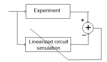 Figure3. Modification of the linearized transistor model parameters is directed by experiments or in comparison with the simulation of the original circuit.
In our proposed methodology the process is done in two steps. First, the circuit is manually linearized by replacing the transistors with their linear model parameters that are best available for the region of operation and the bandwidth specified. We next simulate the linearized circuit as well as the original analog circuit and then compare the two results. If the responses happened to be close enough then we have hit the target, and the model parameters have been rightly selected. Otherwise, we go through the second step, in which we select one of the model elements in the circuit that seems most effective in changing the output response. Then we will proceed into a procedure that tries to modify the model element aiming at a response that mimics the response from the original circuit.
All we are trying to do in this methodology is to focus on this second step of the process, and find the right model component for the transistor. In case one selected model element does not finish the job to our satisfaction, we can still follow the same procedure with another model component. This is well illustrated in Fig. 3. As shown, the experimental results getting from a spectrum analyzers or a digital oscilloscope are compared with the results coming from simulating the linearized circuit. Alternatively, both the original circuit and the linearized one can be simulated in combination. Now, if the two responses are still too far apart the difference is fed back into the system to further modify the selected model component in the linear circuit. This is a sort of an ad hoc adaptation procedure. The question is, what is the purpose of manually linearizing an analog circuit when we don’t have the exact model parameters for its transistors? Or what are the advantages of linearizing a circuit when we do not have access to the accurate model parameters? The answer to these questions mainly rely on the simplicity and the analytical power that exits with linear circuits. The experiments on nonlinear circuits are limited to the conditions and regions that the circuit operates in. After the biasing of the transistors in a nonlinear setting are completed we need to do performance (AC) design. We need to linearize the devices using model parameters that are valid for the selected regions of operations and the bandwidth we need.
So, circuit linearization shifts our circuit analysis and design from nonlinearity into linear domain, with all its properties and advantages. Even if a set of manually selected linearized model parameters are properly working for a certain operating condition then we can claim that we have reached to a regional situation, and in case the operating conditions of the transistors shift to a new region we can still try to modify those parameters again to reach to a solution for the new case. After all, we don’t forget that this is just a simulation and the purpose is to explain the devices behavior in certain regions of operations, and in an educational setting.
Another point worth mentioning here is that, depending on the operational environment, it is most preferred to compare the results of a manually linearized circuit with experiments that are done with the real circuit. This is of course more easily done in case of a laboratory environment, but for a class or study room setting where only simulation facilities are available the case is different. Hence, for the latter case, it is more practical to have both original circuit, as the reference circuit, and the linearized circuit combined in one circuit and then simulate.
2.1. Linear model parameter identification
The type of arrangement just described is illustrated in Fig. 4 for a single model parameter change. Figure 4(a) is a symbolic representation of the linearized circuit along with a selected model element, denoted by P, to be modified. In Fig. 4 (b) the actual circuit, denoted by M, is connected in parallel with the linearized circuit N ready for simulation. The responses of the circuits, i.e., the linearized N and the original circuit M, are then continuously compared. To keep the two responses identical, a nullator is used in the output port. Notice that the nullator, in addition of keeping the two output responses identical, it also provides independence for each circuit to operate without being interfered by the other. In exchange, it is the pairing norator that is responsible to provide the condition needed for such situation.
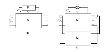 Figure4. (a) Manually linearized circuit N with a variable element P to be added; (b) nullor is added to be able to realize the element P.
Now, there are two cases that might happen. Either the v – i characteristic of the norator closely matches with that of the selected model component or they are way apart. For the former case the experiment is over and the model component remains unchanged for the linearized circuit.
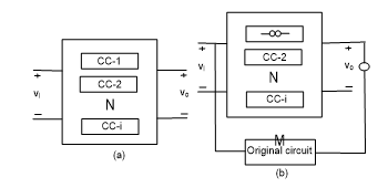 Figure 5. (a) Manually linearized circuit N with one or more possible sub-circuits CC; (b) nullor is added to keep the interconnection between the linear circuit and the original circuit ordered.
In the second case, we find that the model component and the norator do not match, which means we need to modify the model component so that its v – i characteristic is getting close enough to that of the norator. However, it is always possible that a single model parameter (component) may not completely solve the problem. In this situation we need to select another model component and continue with the same process, and so on. This situation is displayed in Fig. 5 with multiple Circuit Components (CCs) to be considered. Again, Fig. 5(a) shows the linearized circuit with i number of model elements, denoted by CC, that are candidates for changes. In Fig. 5 (b), on the other hand, the actual circuit, denoted by M, is added and connected in parallel with the linearized circuit. The rest of the testing procedure is the same as was explained previously. The difference, however, is that here we go through simulations multiple number of times and in each time one of the CC components is replaced with a norator. This certainly continues improving the performance of the linearized circuit in reference to the actual circuit, in multiple steps until we get satisfied with the results.
Now we reach to a point that we can put the entire process into an algorithm for implementation.
Algorithm 1 – Consider a circuit M with transistors. Let M be manually linearized and call the resulted circuit N, as described earlier. We can then go through a stepwise procedure that modifies and corrects one or more model elements of the transistors in order to make the response of the linearized circuit to closely follow the response given by the original (nonlinear) circuit. The rest of the procedure is as follows:
- Search for one or more transistor small signal model elements in N and call them CCj, for all j, as shown in Figs. 4(a) and 5(a). Connect N and M circuits together through a nullator. For now make this connection parallel-parallel (for other possibilities see Footnote 1), as shown in Figs. 4(b) and 5(b).
- Chose one of the model components CCs, say CCj. This is a candidate to be modified for the design. Replace CCj with the paring norator.
- Perform a simulation on the combined circuit, M and N, for AC analysis and for the bandwidth that is specified.
- Assume vj(s) and ij(s) to be the voltage across and the current through the norator CCj, respectively. Then find the equivalent pseudo-impedance zj(s) = vj(s)/ij(s) of the norator, and plot its Bode plot pj for the bandwidth given.
- Next, try to replace the norator CCj with an actual component, or a two-terminal circuit, that ideally has the same impedance zj(s) = vj(s)/ij(s). In case such an ideal case is not reached, find the closest component (or a two-terminal circuit) CCj so that its Bode plot response p’j is close enough to pj, for the given bandwidth.
- Replace the norator (CCj) with the component (or the two-terminal circuit) CCj Next, disconnect M from N circuit, and then simulate N alone for its response.
- If more modifications are still needed, go to step 2 and select a different model component, say CCk in N and follow the rest of the procedure. Continue with the procedure, as many times as needed, until an acceptable response is obtained.
3. Examples
Several examples are worked out here that illustrate the way the proposed method works. Example 1 assumes a circuit with a single nMOS transistor. Instead of using the exact model parameters, given in the data sheets, we simply use level 3 Spice model for long channel devices with values most appropriate. Next, we try to modify the parameter values until we get close enough to the desired response. To do this we use the FNP technique, described before, to adjust the model parameters within the bandwidth specified. Example 2 is given for a two stage nMOS amplifier with multiple transistors, where the type and size of the transistors are the same as those in Example 1. Therefore, we should be able to utilize the same transistor model parameters developed for Example 1. Example 3 is yet another nMOS transistor amplifier that utilizes FNP technique to modify the transistor model parameters. Here also we keep our previous level 3 transistor model used in Examples 1 and 2 unchanged. The point of repeating the same model for all three cases is to see how expanding the circuits with more transistors but with the same transistor linear modeling affects the accuracy and the validity of the proposed method.
Example 1: – Take a single stage MOS amplifier, as shown in Fig. 6(a). Next, proceed to linearize the amplifier by using level 3 model parameters for its transistor. The assumption is that we
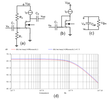 Figure 6. (a) An nMOS transistor amplifier; (b) diode connection; (c) equivalent diode connection in the linearized amplifier; (d) comparing plots for the input impedances in (b) and (c).
have no access to the Spice parameter values at this point, although the simulator is assumed to use the latest device model. To get the pseudo-parameters for our linearized model we go into two operational steps. First, we connect the transistor in a diode format (in the original circuit as well as in the linearized circuit) and then simulate the two circuits combined. Figures 6(b) and (c) are the two circuit schematics, and the Bode plots resulted from the two impedances, looking through the input ports, are demonstrated in Fig. 6(d). Note that for readability purposes one plot is artificially raised by 0.5 dB, otherwise the two are exactly the same.
Now, in the next step we use an FNP (similar to nullor) procedure to find the remaining parts of the model parameters for the transistor. To do that, we can simply use the actual amplifier (Fig. 6(a)) as the “model” circuit to help to adjust the model parameter in the linearized circuit, as given in Fig. 7(a). The Spice circuit code for the combined circuit is also given below, where a voltage controlled voltage source (e1) is used to represent an FNP.
.control
destroy all
set units = degrees
ac dec 1000 1.0e6 1.0e11
plot db(v(3)) db(v(6))+1
.endc
******** Combined circuits *******
Vin 2 0 DC 0 AC 1
x11 2 3 non-Lin
x21 6 2 0 Lin-Mos
************** Circit 2 *********
.subckt Lin-Mos 7 6 0
gm1 7 0 6 0 0.495m
cgs1 6 0 55.8f
*VCVS e1 6 7 3 7 1.0e06
rgd1 6 7 2.2856MEG
cgd1 6 7 9.7f
.ends
***************** Ciruit 1 ******
.subckt non-Lin 3 7
VDD 2 0 DC 5
id1 2 5 20u
M11 5 4 0 0 N_1u L=1u W=50u
r11 4 0 198k
r21 2 4 1MEG
c11 3 4 10u
c21 5 7 10u
.ends
.include cmosedu_models.txt
.end
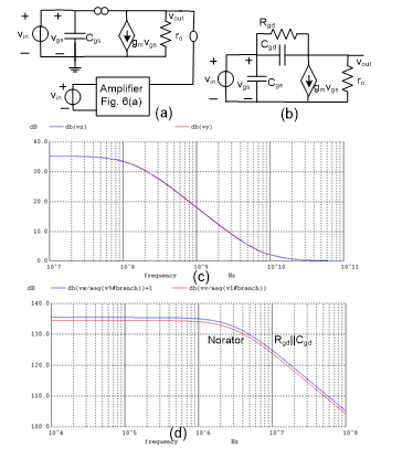 Fig.7. Getting the model parameters for the nMOS; (a) assumsed linearized circuit is parallel with the amplifier circuit; (b) nMOS linear model circuit; (c) gain responses for the actual amplifier and its linear equivalent circuit; (d) plots for the impedance functions, the norator and the replacement with the parallel Rgd and Cgd circuit.
In Fig. 7(c) we notice one gain plot from the actual amplifier and one from the linearized circuit. Obviously the two must be identical because a nullator enforce them to. Next, we need to replace the norator with one or more real component. To find this component we first run the circuit with the norator and make a plot of the impedance function of the norator. This plot is given in Fig. 7(d). The ideal solution is possible if we could find one or more combination of real components that represent the same impedance plot. Here we notice the norator plot is in fact very close to the impedance plot of a parallel RC circuit. This RC circuit is represented by Rgd and Cgd in the linearized circuit given in Fig. 7(b), and the impedance function of the Rgd || Cgd is also plotted in Fig. 7(d), which is almost identical to the norator impedance (except for the 1dB clearance). This concludes our Example 1.
Example 2: – Consider a two stage nMOS shunt – shunt feedback amplifier, as shown in Fig. 8 [12]. There are four identical nMOS transistors used in this amplifier. In order to minimize our modeling efforts, we are going to use the same type and size transistor we used in Example 1. With this choice, to linearize the amplifier circuit all we need to do is to replace each transistor with its linear model already found in Example 1 with a bit of adjustment. This adjustment is done on the resistance rgd, which is in parallel with cgd in the transistor model. The value of rgd in Example 1 was found to be close to 2.3 MEG ohms, whereas in Example 2 it was increased to 40 MEG ohms, where both resistances are quite large anyway. The list of the Spice program for this example is given below.
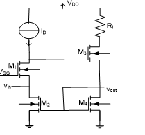 Figure 8. A two stage nMOS current amplifier.
.control
destroy all
set units = degrees
ac dec 1000 1.0e5 1.0e10
plot db(I(v21)) db(I(v31))
plot ph(I(v21)) ph(I(v31))
.endc
****** The combined circuit ******
ii1 0 2 DC 0 AC 1
x11 2 3 Mos-2
x21 2 4 M-Linear
v21 3 0 DC 0
v31 4 0 DC 0
****** Linear circuit ********
.subckt M-Linear 8 9
x11 6 0 3 Lin-Mos
x21 3 4 0 Lin-Mos
x31 7 6 4 Lin-Mos
x41 4 4 0 Lin-Mos
r11 0 6 160k
r21 0 7 100k
c11 3 8 10u
c21 4 9 10u
.ends
*************** Linear-Modeling ********
.subckt Lin-Mos 7 6 3
gm1 7 3 6 3 0.52m
cgs1 6 3 55.8f
rgd1 6 7 40MEG
cgd1 6 7 9.7f
.ends
***************** The original Amplifier ********
.subckt Mos-2 8 9
VDD1 2 0 DC 5
VG1 5 0 DC 1.770833
M11 6 5 3 0 N_1u L=1u W=50u
M21 3 4 0 0 N_1u L=1u W=50u
M31 7 6 4 0 N_1u L=1u W=50u
M41 4 4 0 0 N_1u L=1u W=50u
r11 2 6 160k
r21 2 7 100k
c11 3 8 10u
c21 4 9 10u
.ends
.include cmosedu_models.txt
.end
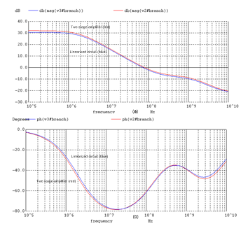 Figure 9. Bode plots given for the gains for the two stage nMOS amplifier and its linearized circuit; (a) magnitude plots; (b) phase plots.
Now it is time to simulate the amplifier and its linearized equivalent circuit in combination. The simulation generates the output transfer functions plots given in Figs. 9(a) and (b), where the plots in (a) represent the magnitude and in (b) the phase angle plots. Notice that the plots are almost identical for the original amplifier and its linearized circuit. Further experiments show that with the body effect removed in this example the two responses become even closer and tighter together.
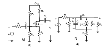 Figure 10. nMOS amplifier circuit and its linearized equivalence. (a) The original nMOS amplifier, and (b) its AC small signal linearized equivalent circuit.
Example 3: – Consider a single stage nMOS amplifier M with feedback, as shown in Fig. 10(a). As usual, we first replace the transistor with its small signal model suitable for this case. This linearizes the amplifier and ready to compare its transfer function with the original amplifier. The model parameters used in this example are assumed to be the Spice Level 3 parameters provided for long channel nMOS transistors. Figure 10(b) shown the amplifier circuit after being linearized.
Our next move it to simulate both circuit, N and M, and plot the transfer functions. Figures 11 represents the plots for (a) the magnitude, and (b) the phase. In comparing the results from the two circuits we notice the differences, particularly in the magnitude plots; although the plots show the same patterns of variations vs the frequency and also in term of poles and zeros locations.
Now the question is what has gone wrong here, and how can this be corrected? In our efforts to find out about this discrepancy we realize that the ratio between the values of the two transistor model capacitors, i. e., Cgs = 2.05 pF and Cgd = 13.83 fF, is very high and close to 150. So, Cgs seems to be too high and must be modified. We pick up Cgs and replace it with a norator, and go through Algorithm 1 for the adjustments.
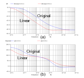 Figure 11. Transfer function responses given for the original amplifier circuit and it linearized equivalent circuit. The differences shown in the responses are mainly the results of mismatch in model parameters. (a) The magnitude, and (b) the phase.
As stated in Algorithm 1, step 2, we are going to make a parallel-parallel connection between the original circuit, M, and the linearized one, N, through a nullor (this connection is the same as that in Fig. 7(a)) and is not shown here. For the norator we choose a current controlled voltage source (CCVS). Next, we use Spice simulation tool to simulate the combined circuit. The partial Spice programming code for this example is given as.
.control
destroy all
let vm1 = v(5)-v(7)
plot db(v(6)) db(v(4))
plot db((vm1)/I(v11)) db((v(8))/I(v31))
.endc
.option scale = 1u
.ac dec 1000 1Meg 100G
VDD1 2 0 DC 5
Vs1 3 0 DC 0 AC 1
**************** The actual amplifier *****************
.subckt model-1 2 3 6
M11 8 5 7 0 NMOS L=2 W=100
ra1 5 0 200k
rb1 2 5 330k
ri1 5 3 100k
r31 2 8 5.1k
r21 7 0 1k
ci1 5 4 10u
co1 8 6 10u
.ends
************** The linearized circuit ****************
ri1 3 5 100k
r21 7 0 1k
rg1 5 0 82k
r31 8 0 5.1k
ro1 8 7 180k
c11 5 7 2.05p
c21 5 8 13.83f
g11 8 7 5 7 1.648m
*********** Circuits combined ****************
x11 2 3 4 model-1
v01 7 4 DC 0
v11 5 b DC 0
h11 b 7 v0 1.0e8
* *********** Testing Bench ***************
v31 3 9 DC 0
rx1 9 a 190
c31 a 0 300f
.include cmosedu_models.txt
.end
We notice from the simulation results that in order for the linearized circuit to respond exactly similar to that of the original amplifier is the followings. We must replace the norator with one or more components that in combination represent an impedance function with the characteristic plot given in Fig. 12(a), plot CC. Now, with a close look at this plot we come to a conclusion that this plot cannot be just from a capacitor Cgs alone. There must be a series combination of a capacitor and a resistor. This is because we see at least one zero on the real axis in the LHP. This RC circuit is shown in Fig. 12 (b), where we find C = 300 fF and R = 190 W. Next, when we plot the impedance function of the RC circuit we come up with the plot RC given in Fig 12(a). As noticed, the two plots, RC and CC, are now so close together, which are almost undistinguishable from each other. Our next move is to replace the norator in N with the RC circuit just found.
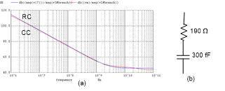 Figure 12. (a) Comparing Bode plots associated with two impedances; one representing the norator (CC), and the other one the RC circuit. (b) The series RC circuit.
After we have made the substitution (i. e., the original model element Cgs = 2.05 pF, is replaced by the components C = 300 fF and R = 190 W in series) we simulate the circuits, this time disconnected from each other, except for the source signal. The frequency responses of both circuits are now plotted in Fig. 13, (a) for magnitude, and (b) for the phase. Comparing the plots in Figs. 13 (a) and (b) with those in Figs. 11 (a) and (b) we see drastic changes. There are much more improvements, and this is particularly evident from the magnitude plots given in Fig. 13(a).
It is of course possible to go one step further and pick up another component in the transistor model for change. The process will be the same as explained before, i. e., replacing the component with a norator first and then follow Algorithm 1 for further processing. The result is expected to get the linearized circuit response closer to that of the original amplifier. However, we think the error is negligible at this point and there is no need to go further.
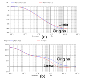 Figure 13. Comparing two transfer functions plots, one associated to the original nonlinear amplifier, and the other one to the linearized equivalent circuit; (a) magnitude, and (b) phase responses.
4. Conclusion
A simple and practical techniques is presented to manually linearize an analog circuit. The method starts with linearizing the transistors based of simple and available models but it gradually modifies one or more model components until an acceptable result is reached.
The method simplifies the case in two steps. First, adopt a most recent model with nominal parameter values for the transistors and simulate the circuit. Second, compare the circuit responses with those getting from the original circuits when simulated or in experiments. Then with the help of one or more nullors modify the manually selected model parameters so that the two responses become close enough for the application. Several examples demonstrate the way the technique works.
The method is especially useful for teaching electronic circuits to students and trainees, where understanding of how linearized modeling of devices works is of prime interest. It is shown that this modeling procedure is completely external to the device and works based on the circuit application and for an assigned bandwidth.
In this procedure the circuit is first manually linearized, which means replacing the transistor with a linear model that is available to the designer. The next step is to combine the linearized circuit with the original circuit in such a way that they behave independently without any interfering each other, but at the same time their responses remains identical. From circuit theory stand point, this is only possible if we allow a component (norator) in the linearized circuit to have varying (v and i) variables. The next step in the process is to replace the norator with a real component or sub-circuit in the transistor model. Evidently, this may not always work quite accurately due to the realizability of the component. In case the result obtained after this substitution is still unacceptable the process can go on including other components of the linearize model. That is, the process of modifying and correcting the manual modeling of the device can continue until the final response we receive is working and acceptable.
- T.L. Pillage, R.A. Rohrer, C. Visweswariah, Electronic Circuit & System Simulation Methods, McGraw-Hill 1995.
- A. S. Sedra, and K. C. Smith, Microelectronic Circuits, Seventh Edition, Oxford University Press, 2015.
- E. Tlelo-Cuautle, Advances in Analog Circuits, InTech, 2011.
- C. Sánchez-López, A. Ruiz_Pastor, R. Ochoa-Montiel, and M. A. Carrasco-Aguilar, “Symbolic Nodal Analysis of Analog Circuits with Modern Multiport Functional Blocks,” Radio Eng., vol. 22, no. 2, pp.518-525, June 2013.
- E. Tlelo-Cuautle, C. Sa´nchez-Lo´pez, E. Marti´nez-Romero, Sheldon X.-D. Tan, “Symbolic analysis of analog circuits containing voltage mirrors and current mirrors,” Analog Integr Circ Sig Process 65:89–95, DOI 10.1007/s10470-010-9455-y, 2010.
- M. Fakhfakh, E. Tlelo-Cuautle, F. V. Fernández, “Design of Analog Circuits Through Symbolic Analysis,” https://books.google.com/books?isbn =1608050955, Computers 2012.
- C. Sánchez-López et al, “Pathological Element-Based Active Device Models and Their Application to Symbolic Analysis,” IEEE Trans. Circuits Syst. I: Regular Papers, vol. 58, no. 6, pp 1382 – 1395, June 2011.
- R. Hashemian, “Application of Fixator-Norator Pairs in Designing Active Loads and Current Mirrors in Analog Integrated Circuits,” IEEE Trans. Very Large Scale Int. (VLSI) Syst., vol. 20, no. 12, pp 2220 – 2231, Dec. 2012.
- R. Hashemian, ” Fixator-Norator Pairs vs Direct Analytical Tools in Performing Analog Circuit Designs,” IEEE Trans. Circuits Syst. II, Exp. Briefs, vol. 61, no. 8, pp. 569 – 573, August 2014.
- R. Hashemian, “Application of Nullors in Designing Analog Circuits for Bandwidth”, IEEE Inter. Conf. on Electro/Information Tech., EIT2016 conference proceedings, Grand Forks, ND, May 19 – 21, 2016.
- R. Hashemian, “Nullors in Finding/Modifying Transistor Parameters, Blindly”, IEEE International Conference on Information and Computer Technologies (ICICT), DeKalb, Illinois, March 23-25, 2018.
- R. J. Baker, CMOS, Circuit Design, Layout, and Simulation, John Wiley &Sons, New Jersey, 2008.
No related articles were found.