Contactless Power and Bidirectional Data Transmission via Magnetic Field

Adv. Sci. Technol. Eng. Syst. J. 3(5), 226–234 (2018);
 DOI: 10.25046/aj030528
At present, the wireless charging and data transmission systems developed by major car manufacturers rely heavily on additional transmission equipment. This paper presents a newly developed wireless power and bidirectional data transmission scheme without adding any radio frequency (RF) devices. The battery charge status and vehicle related information can be transmitted bidirectionally in the wireless manner by the compensation capacitor between two isolated units. Based on the function, this system can quickly inform the user when an emergency event occurs during power transmission. An inverter is used on the primary side of the system, and the generated AC power is transmitted to the load at the secondary side through mutual inductance; the secondary side of the system adjusts the load current to transmit data back. The primary side uses the zero voltage switching (ZVS) method to receive data, and the trimming of the current curve to transmit commands; the secondary side of the system receives commands and uses carrier cycles for decoding. Experimental verification shows applicability of the proposed system.
1. Introduction
The principle of inductive power transfer (IPT) is the mutual magnetic coupling between the transmission windings. It transfers the main power source on the fixed side to a plurality of movable devices by means of the air gap [1]. The issue is becoming popular due to the increasingly global concern of energy conservation. However, most of the previous research tasks only focus on the issue of IPT without considering simultaneous power and data transmission. This research intends to deal with the issue with a novel idea. The paper presented here is an extension of our work originally presented in the 2017 12th IEEE International Conference on Industrial Electronics and Applications [2] by including extended results.
Traditional transferring power is accomplished through the contact of the metal contacts (Plug-In). Although this kind of power transmission can meet most of the requirements, it is inconvenient to be used in many occasions, such as moisture, snow, oil exploitation, and underwater power supply. In order to avoid the shortcomings of contact power transmission, contactless power transfer (CPT) has been developed, which is one of the popular wireless power transfer (WPT) technologies. It has no metal contact and hence avoiding the weakness.
The wireless charging method has been receiving attention over a wide range of industrial and civilian applications in recent years which leads to a variety of utilizations such as contactless electric vehicle charging [3-5], bidirectional IPT system [6-8], electric vehicle and power transmission between grid [9], wireless power and data transmission with fully implantable stimulator [10], portable-telephone charging [11], dynamic charging of electric vehicle [12-13], and wireless power and data transmission system [14].
In literature [7], the proposed IPT system has been applied to vehicle battery charging with high efficiency. Its control loop is composed of external and internal paths, used to handle power control between two sides with an additional wireless transmission equipment to transfer data from the secondary side to the primary side. This design requires better transmission security between two isolation units. The IPT system of [15] uses non-contact technology in the drilling machine, and two sets of windings are used for power supply and data transmission respectively. The design would lead to extra production cost.
The architecture of this research task is the use of a flyback converter, which is used for wireless power and bidirectional data transmission, and adopts ZVS technology to reduce switching loss and EMI noise. The secondary side of the system performs data modulation by instantaneously adjusting load current, and the primary side of the system receives data under ZVS. In addition, the system trims the current transmitting command on the primary side, and the secondary side of the system receives command and decodes data. The authors of [15] proposed a transient load detection method, which mainly uses energy injection and free resonance mode to detect the load. Although a similar approach was used here, wireless power and bidirectional data transmission are the focus of this research. Our design proposes an effective power and bidirectional data transmission solution under the architecture of the IPT system. The technology can be combined with a vehicle positioning system to realize a wireless vehicle charging station as the final goal. As for a practical application in the micro grid, when a driver is charging his/her car, if the charge station can immediately know the voltage, current, power and related information of the charging car, the accident can be effectively managed. Beside of this, if the car is used as a mini power generator, the grid side may identify car ID information and count how much power it contributing to the grid.
2. Description of System
2.1. Circuit Design
This research task considers a wireless vehicle charging system with the function of synchronous power and bidirectional data transmission. The primary side (Grid side) uses a utility power supply (AC 110V / 60Hz). The secondary side (Vehicle side) stores the energy transmitted from the grid side in the vehicle battery. In addition to power transmission, both sides can send and receive messages simultaneously through the same conduction windings. At startup, the primary side of the system performs two steps in sequence, namely payload detection and soft start. First, it detects whether there is a payload on the secondary side of the system. If no payload is detected on the pad’s inductance, the primary side stops power output. If a load is detected, the soft start current will give rise to a preset level, and this mechanism minimizes the inrush current flowing through the switch. The schematic diagram of the proposed system is illustrated in Fig. 1.
The fullback converter adopted here is widely used in AC-DC conversion or DC-DC conversion. Its operational principle is similar to the buck-boost converter. In addition to voltage conversion, there is electrical isolation between the input and output circuits.
The system consists of two circuits that are magnetically coupled to each other. The grid-powered battery charging station (GPBCS) converts the main power supply to direct current through a rectifier and a filter. The transmitter generates power at the primary windings and transmits it to the secondary windings, which is located inside of the vehicle, by mutual inductance to complete the wireless power transfer.
The power switch (MOSFET) N2 at the secondary side has two functions. First, it bypasses the output current and then sends “TX data” such as output voltage and current back to the primary side. The way in which the primary side receives data is to detect the period of the feedback voltage VC. For data communication, when the TX data is received and confirmed by the primary side, the switch (N1) at the primary side sends a command to the secondary side. The current transducer (CT) at the secondary side is connected to the circuit to receive the command.
As can be seen from Fig. 1, the magnetic coupling coefficient and the load quality factor Q of the secondary side are closely related to the mutual inductance M. Its equation is as follows:
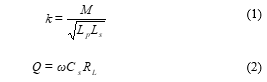 where LP and LS are primary side inductance and secondary side inductance, respectively and CS is secondary side capacitance, RL is load on the secondary side. The operating frequency and rated power of the power supply are mainly limited to the switching components used, both must be balanced according to the copper losses. In this research, the appropriate Q and k were chosen to maintain efficiency of power transmission [5], and S/N ratio, thereby controlling quality of the transmitted data.
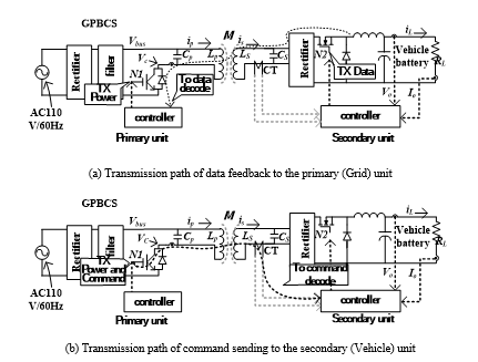 Figure 1. Simultaneous wireless power and bidirectional data transmission scheme
The simultaneous wireless power and bidirectional data transfer system adopts parallel–parallel (PP) reactive power compensation topology. The primary side for parallel compensation is used to generate a large primary current; the secondary side suitable for battery charging current sources [16]. The PP type compensation topology is illustrated in Fig. 2 (a). The topology under mutual inductance coupling can be represented by the simplified circuit depicted in Fig. 2 (b).
As shown in Fig. 2, the impedance reflected from the secondary side back to the primary side is given by
![]() The voltages of the primary windings and secondary windings are expressed as follows:
The voltages of the primary windings and secondary windings are expressed as follows:
 The current of the secondary winding can be expressed by the following equation:
![]() with the resonant frequency of both sides being
with the resonant frequency of both sides being
![]() The secondary side also transmits data to the primary side with the same mutual inductance. The load impedance of the primary side can be known for the network combination of the primary side and the secondary side, namely,
The secondary side also transmits data to the primary side with the same mutual inductance. The load impedance of the primary side can be known for the network combination of the primary side and the secondary side, namely,
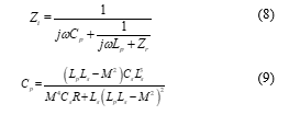
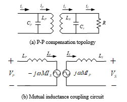 Figure 2. Compensation topology and the simplified circuit
To minimize the VA rating, the imaginary part of the load impedance is adjusted to zero when the secondary side is working at the resonant frequency. The selected primary side capacitance CP is as follows
3. Wireless Data Transmission
3.1. Communication Protocol
The data packet can be divided into four parts, namely start segment, data segment, checksum segment, and stop segment. The entire packet architecture is referenced to the 1-Wire communication protocol and fine-tuned to construct a packet suitable for use with the system. In addition, the universal asynchronous receiver transmitter (UART) specific start segment and stop segment are also retained in the system to separate the packets. The major data types in the data segment are command, voltage value, current value, power, and stop power transmission. The checksum segment is used to detect the entire packet error.
The messages we are about to transmit are divided into two categories based on their attributes. The first category is normal messages including output voltage and current, which is handled with a slower rate. The second category is emergency messages such as overvoltage and overcurrent, which is processed with a faster rate for instantaneous reaction by the system. In addition, when TX data of the secondary side is sent back to the primary side, the system will calculate the charging efficiency. The primary side is the command issuer, which will send the TX cmd to the secondary side. Table I summarizes the specifications for data transmission.
Table 1: Protocol for data transmission
| Category | Baud
rate |
Start
segment |
Data
segment |
Checksum
segment |
Stop
segment |
| Normal
messages |
120 Bd. | 1 bit | 8 bits | 8 bits | 1 bit |
| Emergency
messages |
Operating freq. Bd. | 1 bit | 4 bits | 4 bits | 1bit |
3.2. Data Transmission
When the primary side transmits power to the secondary side, description of data transmission between two sides is explained as in Fig. 3. In this figure, the period between zero-crossing will coincide with the AC line. The time base clock on the primary side is the “Digital AC line” signal generated by the zero-crossing detection circuit. In order to be synchronized with the primary side of the Digital AC line, the secondary side uses a current sensor to measure IS, which is then compared to produce a “Digital IS” signal.
Signal modulation technique is commonly adopted in communication and electronic systems to mix and transmit signals for data transmission in one or more carrier waves. General modulation modes include amplitude-shift keying (ASK), frequency-shift keying (FSK), and phase-shift keying (PSK). In which, FSK has been widely used in digital signal modulation for communication systems such as emergency broadcasts. It uses discrete frequency changes of the carrier to modulate data for transmission. In which, the carry frequency fC is used to discriminate digital “0” or “1”. Referring to Fig. 3, in the preamble section, TOFF of the duty cycle of N2 is fixed. When the secondary side transmits data in the data section, the primary side receives the data in the shadow section; when the primary side transmits the command in the cmd section, the secondary side receives the command in the shadow section.
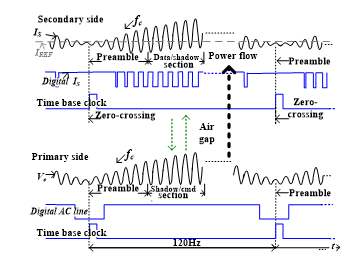 Figure 3. Description of bidirectional data transmission via the mutual magnetic coupling circuits
3.3. Data Decoding
When data is allocated in the data section on the secondary side and modulated to TZ (0), the controller reduces the duty cycle of N2 and the output current (See Fig. 1). The reduced current causes a time delay on the secondary side, which we denote it as . Further, as can be seen from Fig. 4, N2 is turned off in the c-d section so that the current IS flows through the load RL is stored in CS; when N2 works in the d-e section, it is turned on, and CS will discharge to RL. The delayed discharge of CS directly affects VC on the primary side, causing VC to generate a delay time at 0V. At this time, the d-e section corresponding to VC will have a bump. Since N1 operates based on ZVS, the turn on time of N1 is also delayed. The additional delay time produced by the a-e section is also defined as after comparison with the e-g section. The time delay resulting from modulation of the digit “0” is as follows
![]() where TZ (0) under modulation denotes the period of the carrier wave for digit “0” and TC (1) for the digit “1”. The term can be referred to the S/N ratio. An increase in will result in better data transmission quality, making it more robust against noise, and it is more advantageous for the controller on the primary side to decode the signal. However, it might deteriorate the power transmission quality.
where TZ (0) under modulation denotes the period of the carrier wave for digit “0” and TC (1) for the digit “1”. The term can be referred to the S/N ratio. An increase in will result in better data transmission quality, making it more robust against noise, and it is more advantageous for the controller on the primary side to decode the signal. However, it might deteriorate the power transmission quality.
It can be known from the above that the secondary side can send the numbers “0” and “1” by TZ (0) and TC (1) respectively in the data section; the primary side receives the modulated data, which being decoded as “0” or “1” is based on TZ‘ (0) or TC (1). The rule for the primary side distinguishes the digital “0” is determined by
![]() where is a threshold set to identify the digit “0” at the primary side. Illustration of the idea is depicted in Fig. 5 which explains the function for modulating a digit “0” at the center of the data string where curve 1 is IS, curve 2 is the switching state of N2, curves 3 and 4 are the gate voltages of VC and N1, respectively. After changing the duty cycle of N2 (100% adjusted to 94%), it can be seen that the waveform of IS becomes the defined TZ (0); the waveform of the synchronous VC also becomes the defined TZ‘ (0). As can be seen from the results in the figure, when the periods of IS and IP are the same, the operating frequency will be affected when IS changes.
where is a threshold set to identify the digit “0” at the primary side. Illustration of the idea is depicted in Fig. 5 which explains the function for modulating a digit “0” at the center of the data string where curve 1 is IS, curve 2 is the switching state of N2, curves 3 and 4 are the gate voltages of VC and N1, respectively. After changing the duty cycle of N2 (100% adjusted to 94%), it can be seen that the waveform of IS becomes the defined TZ (0); the waveform of the synchronous VC also becomes the defined TZ‘ (0). As can be seen from the results in the figure, when the periods of IS and IP are the same, the operating frequency will be affected when IS changes.
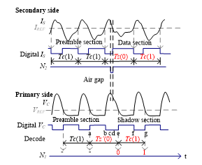 Figure 4. Data decoding method
Fig. 6 shows the varying duty cycle of N2 vs. . It can be seen from the figure that after adjusting the duty cycle, a near linear relationship can be obtained between 85% and 94%. The relationship is as follows:
![]() where the modulated Toff is duty off of N2 for the secondary side to send the digit “0”, the uncertainty is set in our experiments. If the modulated , the primary side decodes data as the digit “0”.
where the modulated Toff is duty off of N2 for the secondary side to send the digit “0”, the uncertainty is set in our experiments. If the modulated , the primary side decodes data as the digit “0”.
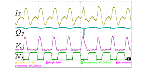 Figure 5. The digit “0” is modulated by reducing the duty ratio of N2 from 100% to 94% when transmission power is at 700 W
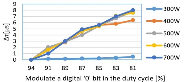 Figure 6. Relationship between duty cycle of N2 and
3.4. Command Transmission
In order to prevent conflicts during data transmission, the system-defined data arrangement string is shown in Fig. 7 where TX cmd is the corresponding command message generated on the secondary side after sending the message on the primary side. The reset time is set to wait for the next string. As for TX data, it is the feedback from the normal message of the secondary side, such as output voltage and current. Fig. 8 depicts how the system processes TX cmd synchronously during the wireless power transfer.
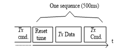 Figure 7. Data transmission scheme
When the system is operating normally and there is no emergency on the secondary side, the primary side places command in the Cmd. section with baud rate 120 Bd. To react, the secondary side detects command accordingly in the shadow section from “Digital IS”. When modulation is performed to the digital “0”, the primary side changes the duty cycle of the switch N1. As seen from Fig. 9, the time required for TON is shorter when modulating “0” and the time required for TON when modulating “1” is longer. The reduced current causes a loss of time on the primary side, which is what we call . Referring to Fig. 8, the primary side will arrange data to be sent in the Cmd. section. The turn on time N1 in the b-c section will be shorter than other parts. The current change of IP will affect the secondary side, which is to be explained later. It causes a reduced time period at the shadow part in the a-d section than that in the d-e section. It can be found from the upper sub-figure of Fig. 8 that the term generating the digital messages “0” is defined as
![]() where denotes the primary side modulating a digit “0” to the secondary side. The secondary side receives command and decodes it to be “0” or “1” depending on TC (1) and . The secondary side distinguishes the digital “0” based on the following criterion:
where denotes the primary side modulating a digit “0” to the secondary side. The secondary side receives command and decodes it to be “0” or “1” depending on TC (1) and . The secondary side distinguishes the digital “0” based on the following criterion:
![]() where denotes the secondary side receiving a digit “0” and Δref is a threshold for judging the digit “0” at the secondary side. If , the primary side trims the duty cycle of N1 as
where denotes the secondary side receiving a digit “0” and Δref is a threshold for judging the digit “0” at the secondary side. If , the primary side trims the duty cycle of N1 as
![]() where and are defined as above. If , the secondary side decodes data as the digit “0”. Figs. 10 and 11 display the function for modulating a digit “0” ( ) at the center of the data string. It is seen that , by modulating the duty cycle of N1, is relatively shorter than that of modulating a “1” by . Fig. 9 shows simultaneous wireless 700 W power transfer while simultaneously transferring Tx cmd the under the air gap of 25 mm and 0 mm lateral offset.
where and are defined as above. If , the secondary side decodes data as the digit “0”. Figs. 10 and 11 display the function for modulating a digit “0” ( ) at the center of the data string. It is seen that , by modulating the duty cycle of N1, is relatively shorter than that of modulating a “1” by . Fig. 9 shows simultaneous wireless 700 W power transfer while simultaneously transferring Tx cmd the under the air gap of 25 mm and 0 mm lateral offset.
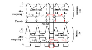 Figure 8. Working mechanism of command transmission
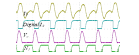 Figure 9. Simultaneous transmission of TX cud at 700 W power transmission (Under 25 mm air gap and 0 mm offset)
3.5. Emergency Message
If there is abnormal voltage or current detected during power transmission, the system will stop charging with the highest priority.
We reduce the duty cycle of N2 from 100% to 94% to generate an additional delay time and to confirm the result. The results are shown in Figs. 10 and 11 for the cases of 400 W or 700 W power transmission. It is seen that the primary side can still correctly decode data whether the IPT system works at low or high power.
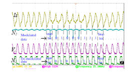 Figure 10. Synchronous transmission of emergency message when transmitting power at 400 W
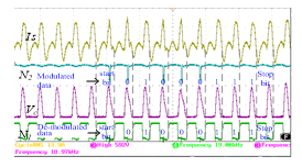 Figure 11. Synchronous transmission of emergency message when transmitting power at 700 W
3.6. Transmission Windings
IPT is a kind of electricity conversion technology. For operation, the primary side windings pass the alternating current IP and the alternating magnetic field intensity H is generated which generates the magnetic flux density ψ via the air medium coupling. This affects the secondary side windings and induces the electromotive force ε (see Fig. 12).
The windings used in this research are the spiral type and the winding ends are not connected. In the real-world experiment, in order to reduce the internal impedance of the windings, the coil has a wire diameter of 2.0 mm to increase the efficiency of transmission. The diameter of the windings is 165 mm, the resonant frequency of the windings is 22 kHz when loaded, and the resonant frequency of the windings is 32 kHz without load.
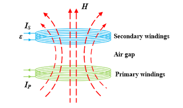 Figure 12. Electromagnetic induction diagram of two transmission windings
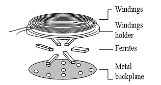 Figure 13. Transmission windings construction used in this research
3.7. Interface
The human machine interface (HMI) control circuit is shown in Fig. 14. It uses the Arduino MEGA 560 as the coordination hub of the entire HMI control circuit, and equipped with an HD44780 universal 16-inch liquid crystal display (LCD) to display the transmission information. The user control interface is implemented by a simple button circuit to facilitate the status display of bidirectional power and data transmission. It communicates with the MCU of the IPT system through a UART communication interface.
The Arduino MEGA 2560 receives the decoded data packet in real time. It also detects the loop of the button instantly. When the user presses the button, it sends a data packet to the IPT system for use by the encoding circuit. Fig. 15 shows the entity of the HMI.
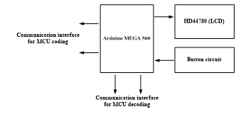 Figure 14. HMI diagram
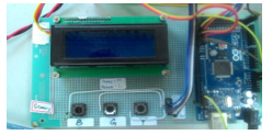 Figure 15. HMI circuit
3.8. Measurement
The primary side controls output power according to the demand of the secondary side. The later simultaneously receives power and measured voltage, current, and power via the way of magnetic field coupling.
The secondary side employs a voltage attenuator and a voltage amplifier to detect charging voltage and current. The crest factor of both signals was designed to equal to 3. These normalized analog signals were connected to a 12-bit ADC device shown as in Fig. 16. In the figure, in addition to measurement, the tasks of the CPU include data encoding, data decoding, and HMI process. To reduce power consumption, the ADC device utilizes the under-sampling method [17-18] to sample signals. It adopts low sampling rate and long measurement period to improve measurement accuracy. The measured raw voltage and current at the sampling time are given by
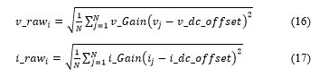
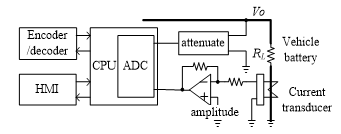 Fig. 16. The secondary control unit with measurement
where N is data update rate, v_Gain and i_Gain are voltage and current gain, respectively. These gains were generated by full-scale calibration. The terms vj and ij are the jth voltage and current sampling values, respectively, v_dc_offset and i_dc_offset are inherent dc-offsets.
Voltage and current are obtained by calculating
 where AVG denotes “average” and K is index of measurement period.
We use the under-sampling approach to measure charging voltage, current, and power. Comparison of the parameters of under-sampling and over-sampling methods is given in Table II. The experimental results are shown in Fig. 17. The measurement error is larger at low output power because of the nonlinear distortion of voltage attenuator and amplifier.
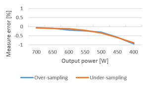 Figure 17. Comparison of the under-sampling and over-sampling methods
Table 2: Measured parameters of under sampling method vs. over-sampling
| Parameter | Sampling type | |
| Under sampling | Over sampling | |
| ADC resolution [bits] | 12 | |
| Crest factor | 3 | |
| Data update rate [ms] | 250 | 250 |
| Sampling rate [kHz] | ≒5 | 200 |
| Measurement period [ms] | 2000 | 250 |
3.9. Efficiency
The primary side controls output power based on the ZVS method. The operational frequency was varied by various output power or demand between 19~30 kHz. The sampling rate was 200 kHz. The channels of sampling voltage and current are Vbus and iP, respectively. Their crest factor is 3. Both signals are connected to the input of ADC and controller for measurement.
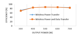 Figure 18. Comparison of efficiency change with output power
Drop of the power transfer efficiency is shown in Fig. 18 when power and data are transmitted simultaneously. As seen from the figure, this will only result in a slight decrease in the power transfer efficiency.
4. Experimental Results
Since the primary side operates at ZVS, the operating frequency of the system can be changed by the load RL. In addition, Q1 on the primary side can have less switching loss and higher efficiency under ZVS operation. If the air gap of two transmission windings changes, the operating frequency of the system will vary. To resolve solve the problem, both units measure the period of TC (1) in the preamble section as a reference.
We conduct the following experiments to verify robustness of data transmission quality (TQ) while there is misalignment between two induction pads or there is load change. We consider Δref to be and parameters listed in Table III. Fig. 19 shows the system hardware and test environment. Power transmission in both sides are controlled by ARM Cortex-M0. The clock speed of the microcontroller is 24 MHz. The data transmission quality (TQ) is defined by
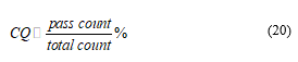 When transmitting a normal message, the total variable count is 1,000. The pass count for the number of correct packets is defined by the following equation:
![]() Data received is treated as a correct message if the checksum (CS) is equal to Data2’s.
Data received is treated as a correct message if the checksum (CS) is equal to Data2’s.
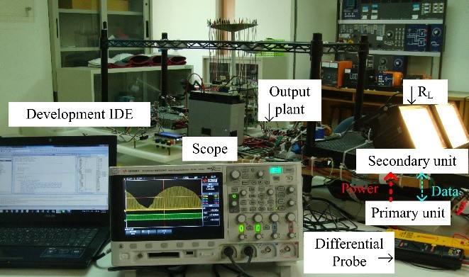 Figure 19. Hardware realization of the IPT system
Fig. 20 presents the result of data TQ. It was recorded by adjusting the lateral shift of two pad’s center from -20 mm to +20 mm. It is found from the experimental results that regardless of the lateral shift between the two pads, an increase in can significantly improve the data TQ. In addition, when the lateral shift of the two pads is maintained within -5 mm to +5 mm, and is set to between to , the data TQ can be as high as 90% or more.
Fig. 21 shows the correlation between output power and data TQ. It can be seen from the figure that communication performance is acceptable (Variation less than 10%) when the system works within 400 W to 700 W and lying between and .
Table 3: Parameters of the prototype IPT system [1]
| Operating frequency | 22 kHz | |
| Windings type | Spiral | |
| Power MOSFET | VDS | 500 V |
| VGS | ±20 V | |
| Rated output power | 700 W | |
| Rated load | 40 Ω | |
| Wire diameter | 2.0 mm | |
| Grid side inductance | 70 uH | |
| Grid side capacitance | 0.35 uF | |
| Grid side induction coil outer diameter | 165 mm | |
| Grid side winding number | 20 turns | |
| Mutual inductance | 26.1 uH | |
| Vehicle side inductance | 69.4 uH | |
| Vehicle side capacitance | 0.35 uH | |
| Vehicle side induction coil diameter | 165 mm | |
| Vehicle side winding number | 20 turns | |
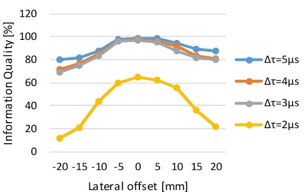 Figure 20. Data TQ for different lateral offsets between two induction pad centers of LP and LS with the nominal air gap 25 mm
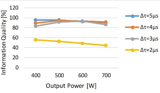 Figure 21. Data TQ vs. output power
Fig. 22 shows that the results of data TQ vs. air gap when the conduction windings LS and LP lies between 15 mm and 25 mm. It is quite clear that performance of data transmission drops quickly when the air gap is greater than 25 mm. However, the experimental results were produced by the prototype sysytem. In general, the optimal air gap of data transmission between two windings may change with charcteristics of the system.
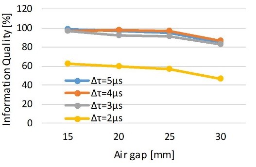 Figure 22. Data TQ vs. air gaps between two induction pads
5. Discussions
While experiments presented in this report demonstrate satisfactory results in either power transmission or data transmission, the power transfer efficiency might drop rapidly due to visible misalignment of two induction pads between vehicle chassis and power station as revealed in Fig. 20. Practically, it is impossible for the driver to move car perfectly so that there is no misalignment between two induction pads. There is a need to develop an adaptive bidirectional wireless power and data transmission control strategy for the optimal TQ under the situation of lateral misalignment between two induction pads. In addition, a clear relationship between data transmission efficiency and physical parameters of the LC tank remains to be investigated.
6. Concluding Remarks
This research report presents a newly developed power and bidirectional data transmission design. The major contribution is that the state of charge of the vehicle battery and vehicle ID information could be mutually communicated through two contactless units. The design exhibits several advantages. For example, the primary (Grid) side of the system can control the output current and achieve steady-state compensation of the secondary (Vehicle) side of the system by wireless transmission. In addition, it costs relatively less while compared with blue tooth or other RF communication technologies because no extra data communication device devices needed. Most importantly, it is a kind of transmission via magnetic field, therefore, there is no serious issue on EMC/EMI. That is, the system is robust against RF interference which makes it to be applicable in the indoor parking lot. To verify applicability, experiments have been conducted with different lateral offsets and vertical shifts between two induction pads which demonstrates performance robustness in power and data transmission.
Acknowledgment
This work was also supported in part by the Innovation and Development Center of Sustainable Agriculture (IDCSA) under the Higher Education Sprout Project, Ministry of Education (MOE) in Taiwan.
- J. Dai, D. C. Ludois, “A survey of wireless power transfer and a critical comparison of inductive and capacitive coupling for small gap applications” IEEE Trans. Power Electron., 30(11), 6017-6029, 2015. https://doi.org/10.1109/TPEL.2015.2415253
- C. C. Huang, H. H. Jian, J. J. Kao, C. L. Lin, Y. T. Kuo, “New Design of Wireless Power and Bidirectional Data Transmission” in 2017 12th IEEE Conference on Industrial Electronics and Applications, Siem Reap, 2017. https://doi.org/10.1109/ICIEA.2017.8282873
- X. Qu, H. Han, S. C. Wong, C. K. Tse, W. Chen, “Hybrid IPT topologies with constant current or constant voltage output for battery charging applications” IEEE Trans. Power Electron., 30(11), pp. 6329-6337, 2015. https://doi.org/10.1109/TPEL.2015.2396471
- E. A. Mehdi, K. Chma, J. Stefani, “Rapid-charge electric-vehicle stations” IEEE Trans. Power Delivery, 25(3), pp. 1883-1887, 2010. https://doi.org/10.1109/TPWRD.2010.2047874
- C. H. Ou, H. Liang, W. Zhuang, “Investigating wireless charging and mobility of electric vehicles on electricity market” IEEE Trans. Ind. Electron., 62(5), pp. 3123-3133, 2015. https://doi.org/10.1109/TIE.2014.2376913
- T. Diekhans, R. W. D. Doncker, “A dual-side controlled inductive power transfer system optimized for large coupling factor variations and partial load” IEEE Trans. Power Electron., 30(11), pp. 6320-6328, 2015. https://doi.org/10.1109/TPEL.2015.2393912
- U. K. Madawala, M. Neath, D. J. Thrimawithana, “A power–frequency controller for bidirectional inductive power transfer systems” IEEE Trans. Ind. Electron., 60(1), pp. 310-317, 2013. https://doi.org/10.1109/TIE.2011.2174537
- D. J. Thrimawithana, U. K. Madawala, M. Neath, “A synchronization technique for bidirectional IPT systems” IEEE Trans. Ind. Electron., 60(1), pp. 301-309, 2013. https://doi.org/10.1109/TIE.2011.2174536
- Y. Ma, T. Houghton, A. Cruden, D. Infield, “Modeling the benefits of vehicle-to-grid technology to a power system” IEEE Trans. Power Syst. 27(2), pp. 1012-1020, 2012. https://doi.org/10.1109/TPWRS.2011.2178043
- Q. Xu, D. Hu, B. Duan, J. He, “A fully implantable stimulator with wireless power and data transmission for experimental investigation of epidural spinal cord stimulation” IEEE Trans. Neural and Rehabilitation Eng., 23(4) pp. 683-692, 2015. https://doi.org/10.1109/TNSRE.2015.2396574
- Y. Jang, M. M. Jovanovic, “A contactless electrical energy transmission system for portable-telephone battery chargers” IEEE Trans. Ind. Electron., 50(3), pp. 520-527, 2003. https://doi.org/10.1109/TIE.2003.812472
- S. Jeong, Y. J. Jang, D. Kum, “Economic analysis of the dynamic charging electric vehicle,” IEEE Trans. Power Electron., 30(11), pp. 6368-6377, 2015. https://doi.org/10.1109/TPEL.2015.2424712
- G. R. Nagendra, L. Chen, G. A. Covic, J. T. Boys, “Detection of EVs on IPT Highways” IEEE Emerging and Selected Topics in Power Electron., 2(3), pp. 584-597, 2014. https://doi.org/10.1109/JESTPE.2014.2308307
- T. Bieler, M. Perrottet, V. Nguyen, Y. Perriard, “Contactless power and information transmission” IEEE Trans. Ind. Electron., 38(5), pp. 1266-1272, 2002. https://doi.org/10.1109/TIA.2002.803017
- Z. H. Wang, Y. P. Li, Y. Sun, C. S. Tang, X. Lv, “Load detection model of voltage-fed inductive power transfer system” IEEE Trans. Power Electron., 28(11), pp. 5233-5243, 2013. https://doi.org/10.1109/TPEL.2013.2243756
- C. S. Wang, O. H. Stielau, G. A. Covic, “Design considerations for a contactless electric vehicle battery charger” IEEE Trans. Ind. Electron., 52(5), pp. 1308-1314, 2005. https://doi.org/10.1109/TIE.2005.855672
- C. S. Wang, G. A. Covic, O. H. Stielau, “Power transfer capability and bifurcation phenomena of loosely coupled inductive power transfer system” IEEE Trans. Ind. Electron., 51(1), pp. 148-157, 2004. https://doi.org/10.1109/TIE.2003.822038
- Y. Liu, J. J. Yan, H. T. Dabag, P. M. Asbeck, “Novel technique for wideband digital predistortion of power amplifiers with an undersampling ADC” IEEE Trans. Microw. Theory Techn., 62(11), pp. 2604-2617, 2014. https://doi.org/10.1109/TMTT.2014.2360398