Analysis of Drain Current Transient Response of Gate Pulse Voltage in AlGaN / GaN High Electron Mobility Transistors

Adv. Sci. Technol. Eng. Syst. J. 3(5), 216–219 (2018);
 DOI: 10.25046/aj030526
Recently, several studies focus on a GaN material system that exhibits a significant probability of use in power devices including wide-gap semiconductors. However, the GaN-HEMT is also a structure that easily leads to crystal defects in AlGaN and i-GaN heterojunction. The aim of the study involved investigating the cause of the current collapse in GaN-HEMT after device construction. A GaN-HEMT with a field plate structure was subject to an environmental temperature change from 300 K to 400 K. A pulse voltage was applied to the gate electrode, and the transient response characteristic of the drain current was analyzed. Given the application of the pulse voltage on the gate electrode, charging and discharging of 2 DEG carriers was repeated with respect to crystal defects near the gate electrode. The charge / discharge reduction was observed via a sampling oscilloscope as a transient response. The transient response exhibited an evident dependence on temperature change. The dependence indicated a time constant change, and thus it was possible to calculate the activation energy of crystal defects trapping carriers. The results suggested that the crystal defect evaluation of GaN-HEMT was possible via transient response analysis of 2DEG carrier by using the proposed method.
1. Introduction
The study is an extension of a previous study originally presented in TENCON 2017 [1]. Recently, several studies focus on GaN material system that exhibits a significant probability of use in power devices with respect to wide-gap semiconductors [2]. The GaN exhibits high breakdown voltage characteristics derived from the wide gap structure, and it is possible to exhibit an output exceeding 1 A in the HEMT structure [3]. Extant studies investigated the application of GaN-HEMTs to green ICT systems as high efficiency devices [4]. The device structure of GaN-HEMT is constructed with a superlattice structure of AlGaN and i-GaN. The superlattice structure exhibits a piezo effect and spontaneous polarization effect and generates two-dimensional electron gas at the interface between AlGaN and i-GaN [5]. Thus, a transistor layer that exhibits a low ON resistance is obtained by constructing a channel layer in GaN that should originally correspond to a high resistance material. Therefore, the GaN-HEMT is a power device exhibiting high withstand voltage, high power operation, and low ON resistance. It is expected that it can be potentially utilized in a wide range of applications including power amplification mechanism of mobile phone base station, power units of artificial satellites, and sensor applications in server power supply [6].
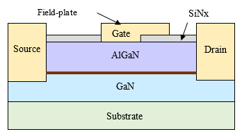 Figure 1 Cross section of the GaN HEMT used in this study.
However, the GaN-HEMT is also a structure that easily causes crystal defects in AlGaN and i-GaN heterojunction [7]. A current collapse phenomenon occurs wherein 2DEG carriers are trapped in the crystal defect and the transfer current value sharply decreases with respect to DC response characteristics [8]. Measures including the addition of a surface passivation film (SiNx), overhanging the direction of the drain electrode of the gate electrode structure (gate plate), and addition of a recess structure between the gate and drain were adopted with respect to the GaN-HEMT structure to suppress the current collapse phenomenon [9, 10]. However, crystal defects are known to increase due to the energization of the device or extreme environmental temperature change, and this deteriorates device characteristics. Additionally, after device construction, it is difficult to identify crystal defects generated in GaN-HEMT [11].
Therefore, the aim of the study involves investigating the cause of current collapse of GaN-HEMT after device construction. A GaN-HEMT with a field plate structure is subject to an environmental temperature change from 300 K to 400 K. A pulse voltage is applied to the gate electrode, and the transient response characteristic of the drain current was analyzed. Given the pulse voltage applied to the gate electrode, charging and discharging of 2 DEG carriers are repeated with respect to crystal defects near the gate electrode. The charge / discharge reduction is observed with a sampling oscilloscope as a transient response. The transient response exhibits an evident dependence on the temperature change. The dependence indicates a time constant change, and thus it is possible to calculate the activation energy of crystal defects trapping carriers. The results suggest that the crystal defect evaluation of GaN-HEMT is possible via the transient response analysis of a 2DEG carrier by using the proposed method.
2. Experimental Method
2.1. Target Device
Figure 1 shows the cross section of the GaN HEMT used in the study. The GaN HEMT includes an i-GaN layer built on a SiC substrate as a channel layer. As a characteristic structure of the HEMT, it includes a field plate that extends the drain side of the T-shaped gate. This suppresses the current collapse phenomenon during normal temperature and high temperature operation.
2.2. Experimental Set Up
Figure 2 shows the experimental diagram in the experiment. In the experiment, the gate voltage was pulsed, and the change in the drain current is observed via a sampling oscilloscope. The base voltage of the gate pulse is set to 0 V, and the rectangular wave pulse is set at the peak voltage of 2 V. The period is 50 ms, and the duty ratio is 0.5. The drain voltage is variable at 0 to 7 V, and the response characteristic observation is set at 3 V. Pulse response characteristics are observed via a sampling oscilloscope (HP83480A, Max: 50 GHz). In order to observe environmental temperature changes, AlGaN / GaN HEMT (Devise under the Test: DUT) is introduced into a nitrogen furnace. The environmental temperature change ranges from 296 K to 373 K. All measurement systems are high frequency compatible (50 GHz).
3. Experimental Results
Figure 3 shows the I-V characteristics of the GaN-HEMT used in the experiment. The blue line in the figure shows the result when only DC voltage is applied. The orange line is obtained by adding high frequency to the gate electrode portion. In the case of only DC voltage, the linear region characteristic of the FET is confirmed immediately after the drain voltage is applied. However, when the drain voltage is 0.2 V or more, the current collapse phenomenon appears, and the current value plummets. When a high frequency component is applied to the gate electrode portion, the carrier trapping effect possessed by crystal defects near the gate electrode is suppressed by the field plate effect, and an almost normal I-V characteristic is obtained. The phenomenon was interpreted as the self-heating of GaN-HEMT in previous studies [12].
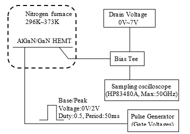 Figure 2 Experimental diagram in this experiment.
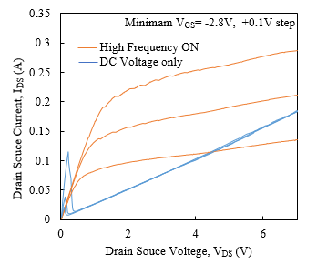 Figure 3: I-V characteristics of the GaN-HEMT.
Figure 4 shows the time axis response of the drain current when a pulse voltage is applied to the gate electrode portion. The time axis response characteristic in nine points in 10K increments from and Figure. 4 (b) shows the enlarged view of the peak portion where temperature dependence is confirmed. As shown in figure 4 (a), three types of peak responses are confirmed. Peak 1 in figure 4 (a) in the temperature dependence is not observed. While a gate pulse voltage is applied, a stable 2DEG current exists under the gate, although the 2 DEG current value plummets at the moment
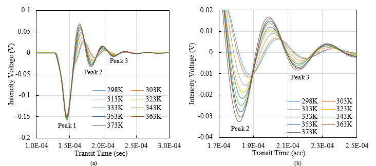 Figure 4 Time-axis response to the drain pulse voltage of the AlGaN/GaN HEMT.
(a) Overall view (b) Enlarged view of peak 2 and peak 3
when the pulse voltage switches to the OFF-State. The peak 1 does not exhibit temperature dependency, and it is considered as a response characteristic when the 2DEG carrier is directly swept from under the gate.296 K is observed by applying a temperature change of up to 373 K. Figure. 4 (a) shows the overall view of the time axis response,
However, peak 2 and peak 3 exhibit an evident temperature dependence as shown in Figure. 4 (b). The temperature dependence in this case exists in terms of both the peak height and peak shape. The peak height indicates the temperature dependence of the number of carriers based on the peak. The peak shape indicates the carrier sweeping process. When the horizontal axis is considered on the time axis, it is interpreted as a transient response. Thus, the shape change indicates a time constant change that limits the transient response. This is discussed in the next section.
4. Discussions
Peak 2 exhibited an evident temperature dependence. The peak height of Peak 2 decreased with increases in the temperature. The peak height was the response voltage and is dependent on the number of carriers. It was considered that the increases in temperature strengthen the piezo effect and increase the thermal carrier supplied from the semiconductor hetero interface. Both the 2 DEG carrier supplied by the voltage and the carrier supplied by the heat were trapped in crystal defects in the AlGaN. The trapping probability was based on the number of carriers wherein thermal carriers increase with increases in the temperature and the number of carriers accumulated in crystal defects also increases [13]. It was considered that the captured carrier is emitted from crystal defects by turning the gate pulse voltage as OFF-State. The emission phenomenon was interpreted as a peak response shown in Figure 4, and transient response characteristics were analyzed.
The response time constant was calculated from the transient response characteristic. As shown in Figure 5, the response time constant decreased with increases in the temperature. Based on the temperature dependence, an Arrhenius plot was executed, and the activation energy ΔE of transient response characteristics was calculated from the slope of the plot. Additionally, ΔE was calculated as approximately 0.575 eV. The value was extremely close to the activation energy of crystal defects in reference [13]. Thus, the transient response indicated by the peak 2 was interpreted as a carrier discharge phenomenon trapped in the crystal defect of the AlGaN layer under the gate.
A pulse voltage was applied to the gate electrode, and thus it was possible to repeat the process of generating / extinguishing the 2 DEG directly under the gate electrode. When only 2DEG carrier generating / extinguished (as shown in Figure 4), peak 2 and peak 3 based on the temperature were not confirmed. When the pulse voltage corresponded to the ON-State at the gate electrode, the 2 DEG carrier was formed under the gate. At the same time, the 2DEG carrier was trapped by crystal defects present in the AlGaN layer near the gate electrode. When the gate pulse voltage turned OFF-State, the 2 DEG carriers were first swept, and the peak 1 was confirmed. There was no reason to observe the temperature dependence in this case. Subsequently, the carriers trapped in crystal defects were gradually released, and peak 2 and peak 3 appeared as transient responses.
We attempted the same analysis for peak 3 although the number of trap carriers was not sufficiently acquired, and the peak intensity was low. An evident temperature dependence was confirmed as shown in the shape in Figure 4. However, an effective analysis result was not obtained. Evidently, the response time of peak 3 was slower than that of peak 2. Additionally, the peak height was lower than that of peak 2. Given that the carrier trap to the crystal defect formed peak 3, a period of time elapsed in releasing the carrier, and it was considered as the characteristic of the crystal defect in the deep part of the crystal. The possibility was considered wherein the presence of crystal defects in the i-GaN crystal depth builds a channel layer [14].
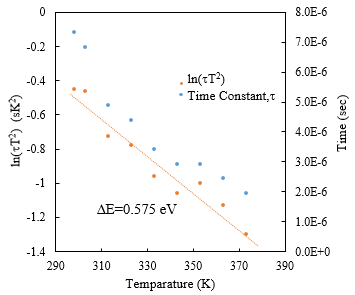 Figure 5 Arrhenius plot using the time constant.
In the study, a pulse voltage was applied to the gate electrode of the completed GaN-HEMT, and the transient response change of the drain current was precisely observed and analyzed. This was a simple method. However, it enabled the evaluation of crystal defects in the completed GaN-HEMT. Although the ICTS method and the DLTS method were used for the same analysis, the method was an extremely simple method when compared with the aforementioned methods and exhibited excellent versatility.
5. Conclusions
The aim of the study involved investigating the cause of current collapse of GaN-HEMT after device construction. A change in the environmental temperature from 296 K to 373 K was applied to GaN-HEMT with a field plate structure. A pulse voltage was applied to the gate electrode, and the transient response characteristic of the drain current was analyzed. Given the application of the pulse voltage to the gate electrode, charging and discharging of 2 DEG carriers was repeated with respect to crystal defects near the gate electrode. The charge / discharge reduction was observed with a sampling oscilloscope as a transient response. The transient response exhibited an evident dependence on temperature change. The response time constant is calculated from the transient response characteristic. As shown in Figure 5, the response time constant decreased with increases in the temperature. Based on the temperature dependence, an Arrhenius plot was executed, and the activation energy ΔE of transient response characteristics was calculated from the slope of the plot. Additionally, ΔE was calculated as approximately 0.575 eV. The value was extremely close to the activation energy of crystal defects in extant studies. The dependence indicated a time constant change, thereby facilitating the calculation of the activation energy of crystal defects trapping carriers. It was suggested that the crystal defect evaluation of GaN-HEMT is possible via transient response analysis of 2DEG carrier by the method.
Acknowledgment
The authors are grateful to the Chukyo University Research Foundation for financial assistance.
- A. Otake, S. Nakano, K. Yamanaka, H. Taguchi, “Temperature dependence of drain current transient response by gate pulse voltage in AlGaN / GaN high electron mobility transistors” TENCON 2017 IEEE Region 10 Conference, Penang, Malaysia, 2017. https://doi.org/ 10.1109/TENCON.2017.8228128
- S. Nakamura, T. Mukai, M. Senoh, “Candela-class high-brightness InGaN/AlGaN double-heterostructure blue light-emitting diodes” Appl. Phys. Lett. 64(13), 1687–1689, 1994. https://doi.org/10.1063/1.111832
- G. Nishio, K. Nakatani, T. Ishizaki, “Design of harmonic processing circuit for microwave GaN-HEMT power amplifier”, IEEE International Meeting for Future of Electron Devices, Kansai (IMFEDK), Kyoto, Japan, 2015. https://doi.org/10.1109/IMFEDK.2015.7158583
- R. Quay, D. Schwantuschke, E. Ture, F. van Raay, C. Friesicke, S. Krause, S. Müller, S. Breuer, B. Godejohann, P. Brückner, “High-power microwave GaN/AlGaN HEMTs and MMICs on SiC and silicon substrates for modern radio communication” Phys. Status Solidi A, 215(9), 1700655(1–7), 2018. https://doi.org/10.1002/pssa.201700655
- K. Shinohara, C. King, A. Carter, E. Regan, A. Arias, J. Bergman, M. Urteaga, B. Brar “GaN-based field-effect transistors with laterally gated two-dimensional electron gas” IEEE Electron Device Letters, 39(3), 417–420, 2018. https://doi.org/10.1109/LED.2018.2797940.
- H. Watanabe, T. Fukami, H. Saito, A. Tomiki, O. Ceylan, H. Nunomura, O. Shigeta, T. Shinke, K. Kojima, “High speed downlink system for small satellite and high-efficiency x-band GaN SSPA” IEEE MTT-S International Microwave Symposium (IMS2014), Tampa, FL, USA, 2014. https://doi.org/10.1109/ MWSYM.2014.6848670
- H. Sasaki, T. Hisaka, K. Kadoiwa, T. Oku, S. Onoda, T. Ohshima, E. Taguchi, H. Yasuda, “Ultra-high voltage electron microscopy investigation of irradiation induced displacement defects on AlGaN/GaN HEMTs” Microelectronics Reliability, 81, 312–319, 2018. https://doi.org/10.1016/j.microrel.2017.10.005.
- H. Huang, Y. Liang, G. Samudra, T. Chang, C. Huang, “Effects of gate field plates on the surface state related current collapse in AlGaN/GaN HEMTs” IEEE Transactions on Power Electronics, 29(5), 2164–2173, 2013. https://doi.org/ 10.1109/TPEL.2013.2288644.
- W. Waller, M. Gajda, S. Pandey, J. Donkers, D. Calton, J. Croon, S. Karboyan, J. Šonský, M. Uren, M. Kuball, “Impact of silicon nitride stoichiometry on the effectiveness of AlGaN/GaN HEMT field plates” IEEE Transactions on Electron Devices, 64(3), 2017. https://doi.org/10.1109/TED. 2017.2654800
- D.Čučak, M. Vasić, O. García, J. Oliver, P. Alou, J. Cobos, A. Wang, S. Martín-Horcajo, M. Romero, F. Calle, “Physics-based analytical model for input, output, and reverse capacitance of a GaN HEMT with the field-plate structure” IEEE Transactions on Power Electronics, 32(3), 2017. https://doi.org/10.1109/TPEL.2016.2569404
- S. Huang, Q. Jiang, S. Yang, C. Zhou, K. Chen, “Effective passivation of AlGaN/GaN HEMTs by ALD-grown AlN thin film”, IEEE Electron Device Letters, 33(4), 516–518, 2012. https://doi.org/10.1109/LED.2012.2185921.
- C. Wang, Y. Xu, X. Yu, C. Ren, Z. Wang, H. Lu, T. Chen, B. Zhang, R. Xu, “An electrothermal model for empirical large- signal modeling of AlGaN/GaN HEMTs including self-heating and ambient temperature effects” IEEE Transactions on Microwave Theory and Techniques, 62(12), 2014. https://doi.org/10.1109/TMTT.2014.2364821.
- M. Mielenz, J. Brox, S. Kahra, G. Leschhorn, M. Albert, T. Schaetz, H. Landa, B. Reznik, “Trapping of topological-structural defects in Coulomb crystals” Phys. Rev. Lett. 110, 2013. https://doi.org/10.1103/ PhysRevLett.110.133004.
- J. Joh, J. Alamo, “A current-transient methodology for trap analysis for GaN high electron mobility transistors”, IEEE Trans. On Electron Devices, 58(1), 132–140, 2011. https://doi.org/10.1109/TED.2010.2087339.