An Experimental Investigation of Reconfigurable UWB Modified Octagonal Microstrip Monopole Patch Antenna with Switchable and Tunable Band-Notched Characteristic

Adv. Sci. Technol. Eng. Syst. J. 3(5), 207–215 (2018);
 DOI: 10.25046/aj030525
An experimental investigation of reconfigurable ultra-wideband (UWB) modified octagonal microstrip monopole patch antenna with switchable and tunable band-notched characteristic is presented in this paper. Notched-bands are obtained by connecting or disconnecting the open shunt stubs. The switching is achieved by using PIN diodes. Additionally, more notch-bands are created by adding additional stubs to the original design and tuning is achieved by employing a varactor diode in the circuit. The proposed antenna has more freedom to suppress the interfering bands because of tuning nature. The proposed designs are simulated, fabricated and then tested. The proposed structures are simple in geometry and useful to operate in the rich electromagnetic scattering environment.
1. Introduction
In today’s world, wireless communication system becomes an essential need for communication. It requires an antenna that must be effective to change its characteristics in reversible manner and it can be utilized for many applications and functions. With the help of transformable antenna, we can replace multiple antennas by a single antenna element which can utilize the complete unlicensed ultra-wideband (UWB) [1]. On this ground, Planar UWB antennas are in great demand [2-7]. While using the entire bandwidth of UWB, other signals that exist in wireless communication system like Worldwide Interoperability for Microwave Access (WiMAX), wireless local area network (WLAN), X-band downlink, X-band satellite communication link, X-band aeronautical radio navigation, etc., operating around 3.5, 5, 5.8, 7.5, and 9 GHz band, respectively, can cause interference. To mitigate this issue, band-notched UWB antennas have been designed that can filter out interfering frequency and improved selectivity. The band-notched UWB antennas have been presented in the past few years.
By inserting a proper slots or slits with different shapes in a radiating element, notched-band can be achieved [3]. In [4, 5], one notch is created while in [7, 8, 9, 10, 11, 12] two notched-bands are obtained. In [13], notched-band has been created by using electromagnetic band-gap (EBG) structure. In [14], one notch band is achieved from CPW-fed monopole antenna, but the structure is compact. Wide notch bands have also been achieved in [15]. Besides this, antenna with static feature will become obsolete for next generation wireless systems. Antenna with reconfigurable feature can be a good candidate for these systems. Reconfigurable antennas have been created by connecting and disconnecting different conducting elements to the main geometry with the help of electrical switches like radio frequency micro-electro-mechanical systems (RF MEMS), PIN diodes or by other methods. Reconfigurability can also be achieved with optical switch or by using material change [16]. A reconfigurable UWB antenna with tuning notched-bands could be advantageous in the future wireless communication systems. Variable notched frequency bands have been achieved in [17], [18]. Some compact UWB monopole antennas reported in the literature can be integrated in a compact system and save space [19], [20]. A reconfigurable UWB modified octagonal monopole microstrip patch antenna with switchable and tunable notched-bands is discussed in this paper. The work proposed in this paper is an extended work originally presented in [21]. The proposed antenna has more freedom to suppress the selected bands.
The paper starts with the introduction. Section 2 describes the design of a reconfigurable UWB monopole patch antenna. Section 3 discusses the modified design to create more notched-bands by adding thin stubs. Section 4 presents the tuning in the structure by using a varactor diode and finally concludes the paper with results and discussions.
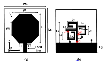 Figure 1. Geometrical model of the modified octagonal patch antenna (a) front side (b) back side.
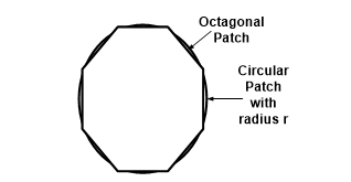 Figure 2. Geometry of a conventional octagonal patch and circular patch
Table 1: Dimensions of the proposed reconfigurable UWB monopole antenna
| Parameter | Value (mm) | Parameter | Value (mm) |
| L | 25.50 | L8 | 04.65 |
| L1 | 04.00 | L9 | 03.30 |
| L2 | 04.00 | Ls | 42.00 |
| L3 | 03.40 | W | 22.50 |
| L4 | 04.23 | W1 | 14.50 |
| L5 | 09.30 | W2 | 00.60 |
| L6 | 05.50 | Ws | 40.00 |
| L7 | 06.60 |
2. Reconfigurable UWB monopole patch antenna design and its operation
2.1. UWB antenna design
The geometrical model of the antenna is illustrated in Figure 1. The antenna is designed on FR4 substrate with relative permittivity of 4.4. The height of the substrate is 1.6 mm. The proposed antenna consists of modified octagonal monopole microstrip patch etched on the upper side and partial ground plane on the lower side of the substrate. Thin metal stubs are etched on the back side of the patch to create notches in the reflection coefficient plot and this is achieved by integrating PIN diodes in the circuit as shown in Figure 1(b). The conventional octagonal (with equal side length) patch is designed by taking its size equivalent to a circular patch as shown in Figure 2. The dominant mode is TM110 (TMmnp), the resonant frequency can be calculated as
![]() Where
Where
c = Speed of light,
r = Radius of the circular patch,
εr = Relative permittivity.
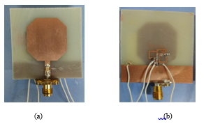 Figure 3. Photograph of a modified octagonal monopole microstrip patch antenna (a) front side (b) back side.
The radius is calculated as 14.05 mm by equating the area of both structures (circular and octagonal patch). The resonant frequency of the dominant mode is 2.94 GHz. The proposed octagonal patch is modified by varying the edges and using partial ground plane and achieved impedance matching throughout the band (3.1-10.6 GHz). The proposed antenna is excited with a 50 Ω line. There are total of three PIN diodes named as D1, D2, and D3 are connected at different places to achieve different notches. PIN diodes are turned ON with the help of biasing circuits at the back side of antenna. The dimensions of the circuit are listed in Table 1. Photograph of the fabricated circuit is shown in Figure 3.
2.2. Operation and results
Three PIN diodes are used to get various states from the circuit. Simulations are done in an EM simulator (Computer Simulation Technology software) [22]. The equivalent model of a PIN diode used in the simulations is shown in Figure 4. The values of Rp, Cp and Rs are 40 kΩ, 0.03 pF and 5 Ω, respectively. The parasitic series inductance is ignored in the simulations. The equivalent model is extracted from the datasheet [23]. Inductors of 56 nH are used to bias the PIN diodes. A capacitor of 100 pF is used in the circuit to block dc. Input impedance of the proposed antenna is plotted in Figure 5. From
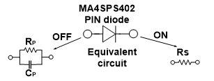 Figure 4. The equivalent circuit model of the PIN diode.
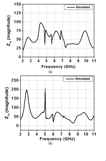 Figure 5. Input impedance of the proposed antenna (a) when all diodes are OFF, (b) diode D1is ON.
Figure 5(a), it is clear that the input impedance lies in the range from 26 Ω to 96 Ω which corresponds to S11 < -10 dB. It is matched in the whole UWB band. Figure 5(b) shows the input impedance of 203 Ω (S11 = – 4.37 dB) at 5.05 GHz and 13 Ω (S11 = – 4.62 dB) at 8.25 GHz, which creates two notches. When all diodes are OFF, the impedance bandwidth is achieved in the range from 2.8 to 11.5 GHz as shown in Figure 6(a). In the second state, diode D1 is turned ON (L5 and L6 stubs are connected to the ground plane); two notched-bands are created around at 5.05 and 8.25 GHz as shown in Figure 6(b). In the third state, all three diodes are ON (all stubs are connected), the notched-bands are shifted to some other bands with centre frequencies of 5.5 and 8 GHz as shown in Figure 6(c) but in this case, the impedance bandwidth is reduced. At 3.1 GHz, the magnitude of reflection coefficient is below -10 dB which is not acceptable.
Further the design is modified to get good impedance match across the whole UWB band except the notched-bands.
3. Modified reconfigurable UWB antenna
The modified structure is shown in Figure 7. The geometry of the top side is same as the previous one; the only change is done on the back side (partial ground plane side). Photograph of the printed design is shown in Figure 8. Two additional stubs are connected in this modified geometry to get more notched-bands. There are 4 PIN diodes in the circuit. Here, measurements are done by taking PIN diode as a metal strip of 0.2 mm × 0.2 mm. Input impedance is plotted in Figure 9. It is perfectly matched in the range 2.8–11.4 GHz. When all four diodes are OFF, the reflection coefficient is below -10 dB across the whole band (3.1-10.6 GHz) as depicted in Figure 10(a). UWB characteristic is achieved from the circuit without turning the diodes ON. In state 2, diode D1 is ON and others are OFF, two notched-bands are created as show in Figure 10(b). In state 3, diodes D1 and D2 are ON, one notched-band is present (around 8.5 GHz) and other notched-band (around 5 GHz) is suppressed because when we connect D2, one more shunt stub (L3 + L4) is connected to the circuit, this open ended stub (length = λ/4) suppress the 5 GHz band as shown in Figure 10(c). In state 4, diodes D1 and D3 are ON, notches are shifted as shown in Figure 10(d), because of change in the effective reactance value. In state 5, diodes D1 and D4 are ON; again, it suppresses the 5 GHz band and obtains the wide notched-band at 7 GHz (center frequency) as shown in Figure 10(e). In the last case (state 6), all diodes are ON, two notched-bands at 3.5 and 7.25 GHz are created as shown in Figure 10(f).
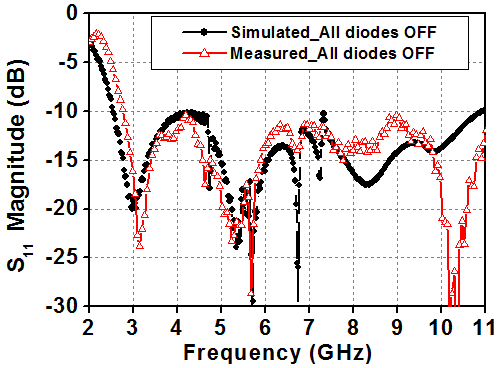
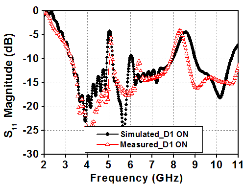
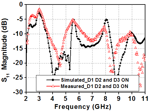 Figure 6. Reflection coefficients of the proposed antenna.
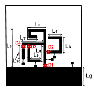 Figure 7. Proposed modified geometry. L3 = 03.40, L4 = 4.23, L5 = 9.30, L6 = 7.10, L7 = 6.3, L8 = 6.2, L9 = 3, L10 = 4.75, Lg = 10.25.
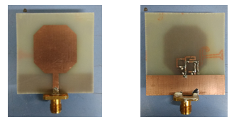 Figure 8. Photograph of the modified geometry in Figure 7.
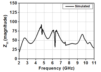 Figure 9. Input impedance of the proposed antenna when all diodes are OFF.
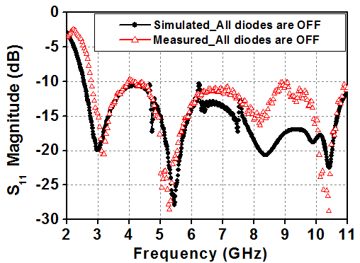
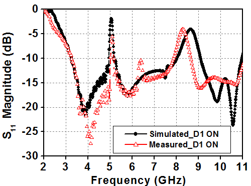
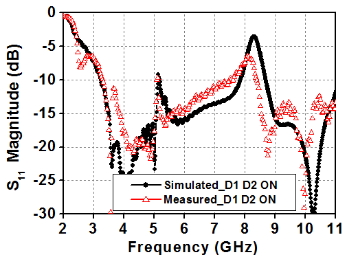
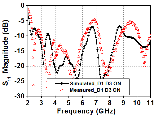
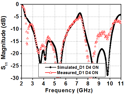
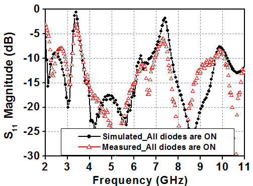 Figure 10. Reflection coefficients of the modified antenna as shown in Figure 7.
4. Switchable and tunable antenna design
The switchable and tunable reconfigurable UWB modified octagonal monopole patch antenna is proposed by modifying the structure as shown in Figure 11. Front side of the structure is same as used in the previous one (Section 2).
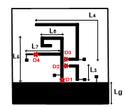 Figure 11. Switchable and tunable notch-band antenna: L3 = 5.1, L4 = 14.8, L5 = 9.45, L6 = 5.5, L7 = 11.2, Lg = 10.3.
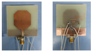 Figure 12. Photograph of the switchable and tunable notch-band antenna as given in Figure 11.
One varactor and three PIN diodes are used to make antenna switchable and tuneable. Photograph of the printed circuit is shown in Figure 12. An input impedance plot, with all diodes OFF, is shown in Figure 13. In the first state, when all diodes are OFF, the reflection coefficient is below -10 dB from 2.94 to 11.85 GHz as shown in Figure 14(a). In state 2, diode D1 is ON, two notched-bands are created at 4.8 and 8.25 GHz as shown in Figure 14(b). In state 3, diodes D1 and D2 are ON, the notched-band created at 8.25 GHz is suppressed by connecting L3 stub as shown in Figure 14(c). In state 4, diodes D1 and D3 ON, notched-bands are shifted
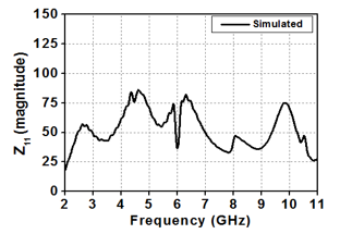 Figure 13. Input impedance of the proposed antenna when all diodes are OFF.
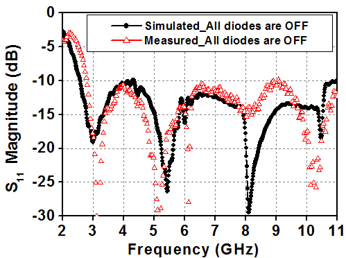
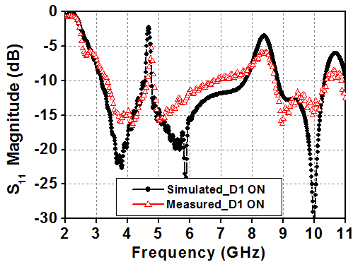
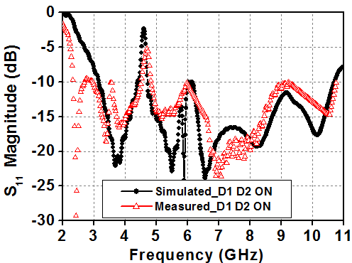
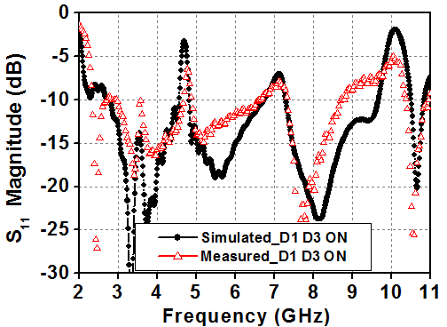
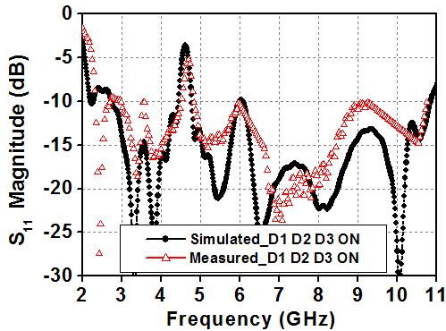
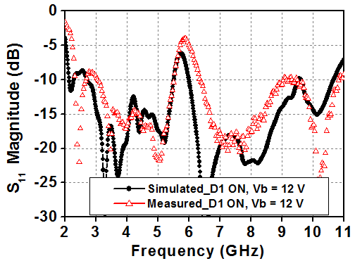
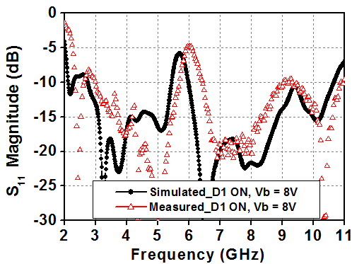
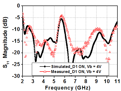
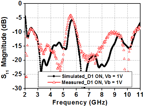 Figure 14. Reflection coefficients of the modified switchable and tunable antenna.
by changing the overall reactance as shown in Figure 14(d). In state 5, diodes D1, D2 and D3 are ON, one notch is obtained at 4.75 GHz as shown in Figure 14(e).
Continuous tuning is also obtained from the structure, diode D4 (varactor diode, model MA46H120) is integrated as shown in Figure 11. Capacitance of the diode varies from 0.1 pF to 1 pF with bias voltage varies from 12 V to 1V, respectively. The results are plotted with different bias voltages as shown in Figure 14(f) to (i). Notch-bands are shifted from higher to lower side with centre frequencies of 6 and 5.5 GHz, respectively.
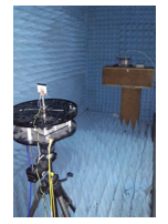 Figure 15. Photograph of the measurement setup.
The radiation patterns of the switchable and tuneable octagonal monopole patch antenna are measured in the anechoic chamber. Photograph of the measurement setup is shown in Figure 15. A double-ridged horn antenna is used to illuminate the test antenna. The proposed (test) antenna is placed on a rotating table which rotates horizontally. Figure 16 shows the normalized radiation patterns. The cross-polarization level is better than 12 dB at all measured frequencies.
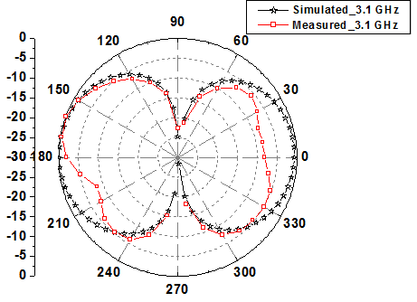
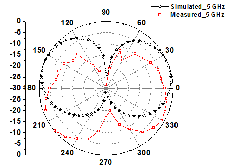
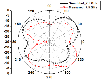
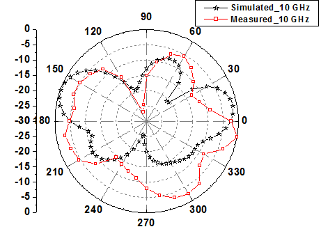
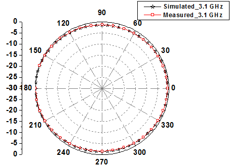
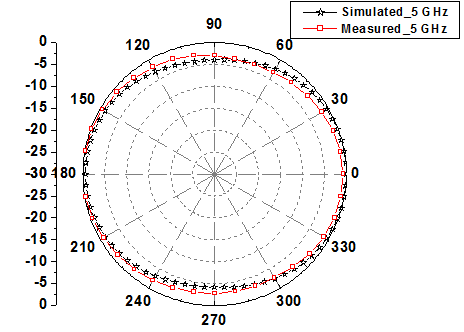
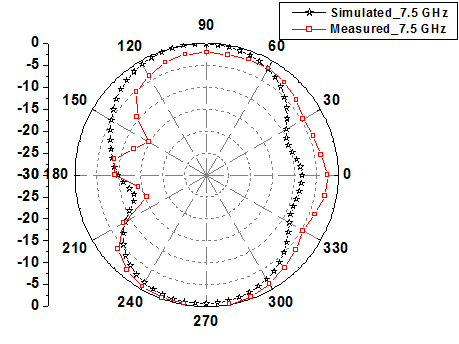
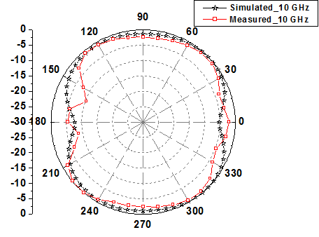 Figure 16. Normalized radiation patterns of the proposed switchable and tunable antenna.
The measured gains are better than 3.12 dB in all states except at the notched-bands. The gains in the notched-bands are below -7.4 dB. The discrepancies in the results are due to fabrication imperfections and use of insulated wires. Insulated wires affect the radiation pattern. Further, the sharp notches can be obtained from this structure by using lumped elements. The filters made from microstrip line have some bandwidth which is more than that of achieved with the lumped elements.
Table 2: Comparisons of the proposed work with earlier reported ones
| Frequency Range (GHz) | No. of notched-bands | Total size L×W
(mm2) |
Type of switching | |
| [9] | 2 – 12.5 | Two notched-bands @ 5.3, 7.4 GHz | 38.5 × 46 | Discrete |
| [17] | 3.1 – 14 | One tuning band @ 5.1-5.9 | 22 × 22 | Continuous |
| [18] | 3.1 – 12* | One tuning band @ 3.6-5.2 | 18 × 21 | Continuous |
| [19] | 2.9 – 12 | Four notched-bands @ 3.5, 4.6, 5.2, 5.8 GHz | 30 × 31 | Discrete |
| [20] | 3.1 – 10.7 | One notched-band @ 5 GHz | 30 × 27.4 | Discrete |
| This work (with varactor diode) | 2.8 – 11.5 | Five discrete notched-bands @ 4.5, 4.75, 4.85, 8.25, 10 GHz and one tuning band @
5.5 – 6 GHz |
42 × 40 | Discrete & Continuous |
* Estimated from the data given in the paper
Comparison with earlier reported papers is given in Table 2. In [9], one quasi-complementary split-ring resonator is etched to achieve dual notched frequency bands while in [20], one notched-band is created by embedding a π-shaped slot in the structure, but the advantage is the compact structure. In [19], four notched-bands are obtained by inserting four U-shaped and one L-shaped slot. Continuous switching was achieved in [17] and [18]. In all these designs except [17], notched-bands were created by perturbing the radiating structure. In this paper, the notched-bands are created by using stubs as band stop filters (BSFs) on the back side of a radiator instead of changing the front side which has a radiator and feed line. In such cases, the radiation patterns are less affected while changing the different states of the antenna [17]. In electromagnetic scattering environment, antenna must have freedom to suppress the selected band. The proposed antenna can suppress the bands with centre frequencies of 4.5, 4.75, 4.85, 8.25, 10 and 5.5-6 GHz.
5. Conclusion
An experimental investigation of reconfigurable UWB modified octagonal microstrip monopole patch antenna with switchable and tunable band-notched characteristic is proposed in this paper. Initially, the design is started with creation of switchable notched-bands, after that some additional notches are obtained by using a modified structure. Finally, by employing a varactor diode, the tuning of notched-bands is achieved. The proposed designs are simple in geometry. The proposed antenna has freedom to suppress many interfering bands. The tunable band-notched reconfigurable UWB antenna is suitable for modern wireless communication systems.
- T. Kaiser, F. Zheng, and E. Dimitrov, “An overview of ultra-wide-band systems with MIMO,” Proc. IEEE, 97(2), 285–312, Feb. 2009.
- J. Ren, W. Hu, Y. Z. Yin, and R. Fan, “Compact printed MIMO antenna for UWB applications,” IEEE Antennas Wireless Propag. Lett., 13, 1517–1520, 2014.
- Wang-Sang Lee, Dong-Zo Kim, Ki-Jin Kim and Jong-Won Yu, “Wideband planar monopole antennas with dual band-notched characteristics,” IEEE Trans. Microw. Theory Tech., 54(6), 2800-2806, June 2006.
- P. Gao et al., “Compact printed UWB diversity slot antenna with 5.5-GHz band-notched characteristics,” IEEE Antennas Wireless Propag. Lett., 13, 376–379, 2014.
- J. -M. Lee, K. -B. Kim, H. -K. Ryu, and J. -M. Woo, “A compact ultra wideband MIMO antenna with WLAN band-rejected operation for mobile devices,” IEEE Antennas Wireless Propag. Lett., 11, 990–993, 2012.
- L. Kang, H. Li, X. Wang and X. Shi, “Compact Offset Microstrip-Fed MIMO Antenna for Band-Notched UWB Applications,” IEEE Antennas Wireless Propag. Lett., 14, 1754-1757, 2015.
- T. K. Roshna, U. Deepak, V. R. Sajitha, K. Vasudevan and P. Mohanan, “A Compact UWB MIMO Antenna With Reflector to Enhance Isolation,” IEEE Trans. Antennas Propag., 63(4), 1873-1877, April 2015.
- J.-F. Li, Q.-X. Chu, Z.-H. Li, and X.-X. Xia, “Compact dual band notched UWB MIMO antenna with high isolation,” IEEE Trans. Antennas Propag., 61(9), 4759–4766, Sep. 2013.
- W. T. Li, Y. Q. Hei, W. Feng and X. W. Shi, “Planar Antenna for 3G/Bluetooth/WiMAX and UWB Applications With Dual Band-Notched Characteristics,” IEEE Antennas Wireless Propag. Lett., 11, 61-64, 2012.
- S. Wei, Y. Yin, Y. Huang, S. Fan, L. Kang and X. Li, “Novel smiling face-shaped antenna for dual band-notched ultra-wideband applications,” 2010 IEEE International Conference on Ultra-Wideband, Nanjing, 2010, 1-3.
- He Huang, Ying Liu and Shuxi Gong, “A novel uniplanar differentially-fed UWB polarization diversity antenna with dual notch bands,” 2015 9th European Conference on Antennas and Propagation (EuCAP), Lisbon, 2015, 1-4.
- D. Yu, G. Xie, Z. Liao and W. Zhai, “Novel dual band-notched omni-directional UWB antenna on double substrates crossing,” 2011 4th IEEE International Symposium on Microwave, Antenna, Propagation and EMC Technologies for Wireless Communications, Beijing, 2011, 95-97.
- L. Kurra, M. P. Abegaonkar, A. Basu and S. K. Koul, “A band-notched UWB antenna using uni-planar EBG structure,” 2013 7th European Conference on Antennas and Propagation (EuCAP), Gothenburg, 2013, 2466-2469.
- X. Wang, Z. F. Yao, Z. Cui, L. Luo and S. X. Zhang, “CPW-fed band-notched monopole antenna for UWB applications,” 2008 8th International Symposium on Antennas, Propagation and EM Theory, Kunming, 2008, 204-206.
- J. Dong, G. Fu, J. Zhao and X. Wang, “Dual band-notched UWB antenna with folded SIRs,” 2012 International Conference on Microwave and Millimeter Wave Technology (ICMMT), Shenzhen, 2012, 1-3.
- A. K. Tagantsev, V. O. Sherman, K. F. Astafiev, J. Venkatesh, and N. Setter, “Ferroelectric Materials for Microwave Tunable Applications,” Journal of Electroceramics, 11, 5-66, 2003.
- R. Zaker, C. Ghobadi and J. Nourinia, “Novel Modified UWB Planar Monopole Antenna With Variable Frequency Band-Notch Function,” IEEE Antennas Wireless Propag. Lett., 7, 112-114, 2008.
- Mahdi Nouri and Sajjad Abazari Aghdam, “reconfigurable uwb antenna with electrically control for triple on-demand rejection bandwidth,” Microwave Optical Technology Lett., 57(8), August 2015.
- Z. H. Wu, F. Wei, X. W. Shi and W. T. Li, “A compact quad band-notched UWB monopole antenna loaded one lateral L-shaped slot,” Progress in Electromagnetics Research, 139, 303–315, 2013.
- Y. -L. Zhao, Y. -C. Jiao, G. Zhao, L. Zhang, Y. Song and Z. -B. Wong, “Compact planar monopole UWB antenna with band-notched characteristic,” Microwave Optical Technology Lett., 50(10), 2656–2658, Oct. 2008.
- Ruchi Paliwal, Rajesh K. Singh and Shiban K. Koul, “Reconfigurable UWB Monopole Antenna with Switchable Frequency Notched Bands,” IEEE Applied Electromagnetics Conference, Dec. 2017, 1-4.
- CST Studio Suite, [Online]. Available: http://www.cst.com/
- Data Sheet of MA4SPS402 PIN diodes, MA-Com, Application Note.