A Novel MICS Receiver with FSK Dual Band Demodulator

Adv. Sci. Technol. Eng. Syst. J. 3(5), 64–71 (2018);
 DOI: 10.25046/aj030509
A low-complexity dual-band chirp FSK, direct conversion receiver is described in this paper. The receiver is dedicated to be used in the transceiver unit of a medical implantable wireless sensor. The system uses the RF band between 402 and 405 MHz. Two sub-bands frequencies employing chirped pulses are assigned for both binary information. The novelty of this work is the use of a Binary FSK LFM modulator, a direct conversion receiver and a simple and low power non-coherent BFSK envelope detection demodulator. Receiver performances are evaluated for all the input power dynamic range. Receiver front-end parameters are optimized using harmonic balance simulation. In order to improve receiver sensitivity, a low pass filter with controllable bandwidth between 40 and 300 KHz is used to avoid in-band interference. The receiver is able to achieve a noise figure of 5.5 dB, a receiver sensitivity of -93 dBm and a maximum data rate of 100Kbps. The simulated IIP3 and P-1dB are 12.6 dBm and 22.1 dBm respectively. A simple non coherent binary dual band FSK demodulator was used which is based on an envelope detector, integrate & dump, a sampling & hold and a liming circuit. The receiver was co-simulated with the dual band non coherent demodulator. The proposed receiver has a sensitivity of -93 dBm and a BER less than 10-3.
1. Introduction
With the proliferation of portable or implantable devices in wireless healthcare sensor network, energy-efficient radios have become an active area of research.
This paper is an extension of work originally presented in International Conference on Engineering & MIS (ICEMIS 2017) [1].
Today, there is a great demand for low power transceivers dedicated to implanted sensors, thanks to the development of new technologies in microelectronics and the progress of sensor implantation techniques in the human body [2]. This system measures certain physiological parameters of people suffering from chronic diseases and communicates useful information to an information collection center in order to warn medical professionals in case of danger [3-5].
The implanted sensor node must provide continuous operation under battery power for at least 5 years.
WMTS (Wireless Medical Telemetry Services) and MICS (Medical Implantable Communications Services) are two standards used for medical electronic devices. Non implantable devices uses WMTS whereas MICS is dedicated to sensor networks implanted in the human body.
According to the MICS regulation from the Federal Communications Committee (FCC) its frequency band is between 402 MHz and 405 MHz which is divided into 10 channels. Each channel occupies a bandwidth of 300 KHz. The wireless communication range is limited to 2 m and the maximum transmitted power is set at -16 dBm [6]. These frequencies were selected for the following reasons: reasonable antenna size, good propagation characteristics for medical implants in the human body and worldwide availability [4].
In addition, MICS signals are safe for the human body thanks to their low power level. Moreover, this introduces low interference with other users. With this technology we can reach reduced complexity, low power and low cost transceiver.
Figure 1 introduces the block diagram of a typical sensor node [7-8]. Physiological signals are very weak and coupled with noise like body pressure or the amount of glucose in the blood of the patient. Thus, amplification and filtering process are required to increase the signal level and reject the noise. A multiplexer is used to switch between different sensors. The analog signal conversion into digital is ensured by an ADC. The microcontroller processes the signals from the sensors unit and executes the communication protocol. The MICS transceiver communicates the formatted data across a wireless link with a portable personal healthcare centre for testing and diagnosis by doctors.
A sensor node can perform communication in both directions. In transmission mode the sensor node sends all the useful sensors data and information regarding its operating status. In receive mode, it receives node configuration, wake up or standby information. It should also be noted that power consumption of a sensor node depends on the duty cycle, the time during which the system is active over a given period.
The use of CMOS technology in healthcare implanted devices is justified since the principal challenge is the minimization of the energy consumption in the sensor nodes in order to integrate the digital and the analog parts together on the same chip. That’s why the architecture of the RF wireless sensors, modulation scheme and parameters optimization of different blocks of the transceiver was subjects of many studies and researches as part of the low power consumption challenge [9].
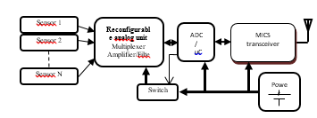 Figure 1. A typical sensor node.
Linear Frequency Modulation (LFM) is widely used in radars, but it has not been yet used for implanted sensor networks in the human body using the MICS band.
The purpose of this paper is to design a simple and low power, 402-405MHz-MICS receiver chain based on the LFM technique with a non-coherent BFSK envelope detection demodulator dedicated for implantable sensor node.
The description of Linear Frequency Modulation technique and transceiver architecture is presented in section 2. In section 3 the receiver design and simulations results will be presented. A co-simulation of the analog receiver with the non coherent dual band FSK demodulator will be shown in section 4. Section 5 presents blocks parameters and performance of the receiver. Section 6 concludes this paper.
2. Chirp FSK MICS modulation
2.1. Mathematical background associated with LFM
Linear Frequency Modulation (LFM) signal or linear chirp modulation signal is considered as a form of spread spectrum technique for wireless communications. Since 1940 chirp modulation has been widely used in radars communication systems because it has the property of pulse compression [9].
LFM has been chosen because it presents performances in terms of distortion, rejection of interference and allows a low power implementation [10]. Linear Frequency Modulation (LFM) signal or linear chirp signal can be representation by (1):
![]() Where the initial frequency of the chirp,
Where the initial frequency of the chirp,
T is the duration of a single chirp pulse and the instantaneous phase varies linearly with time.
The instantaneous frequency is given by (2):
![]() If we make where and are constants then becomes (3):
If we make where and are constants then becomes (3):
![]() We can notice that the instantaneous frequency is a linear function of time with a slope R given by (4):
We can notice that the instantaneous frequency is a linear function of time with a slope R given by (4):
![]() where B is the bandwidth. R is called chirp rate. Therefore the instantaneous frequency is increasing or decreasing over the chirp pulse duration and the bandwidth B equals the swept frequency.
where B is the bandwidth. R is called chirp rate. Therefore the instantaneous frequency is increasing or decreasing over the chirp pulse duration and the bandwidth B equals the swept frequency.
For increasing instantaneous frequency (up chirp) the LFM signal is given by (5):
![]() For decreasing instantaneous frequency (down chirp) the LFM signal can be represented by (6):
For decreasing instantaneous frequency (down chirp) the LFM signal can be represented by (6):
![]() As represented in Figure 2, the transmission of a bit 1 corresponds to the band B1 (402.9 MHz – 403.2 MHz) and the transmission of a bit 0 corresponds to the band B0 (403.2 MHz – 403.5 MHz).
As represented in Figure 2, the transmission of a bit 1 corresponds to the band B1 (402.9 MHz – 403.2 MHz) and the transmission of a bit 0 corresponds to the band B0 (403.2 MHz – 403.5 MHz).
2.2. Transceiver architecture
The super heterodyne architecture presents problems associated with the use of several frequency transposition stages, such as the image frequency that must be taken into account during the design of the receiver. Moreover, this architecture needs an external IF filter which is a major problem to full integration.
In order to avoid image interference, the choice of the receiver architecture was the direct conversion (or zero IF) receiver. In zero IF architecture we can ensure the hardware minimization because it eliminates the image–reject filter and other IF components. Except Low Noise Amplifier (LNA) all amplification and filtering will take place at very low frequencies. Therefore, it is suited to a monolithic integration.
A Linear Frequency Modulation with Binary FSK scheme is proposed for this sensor node. This modulation has advantages over other techniques such as OOK and PPM. The reasons are: the demodulation operation are simple because it demands a zero threshold detector for the decision circuit and it is less affected by inter-pulse interference (IPI) for the same pulse rate [11].
The only disadvantage is that quadrature local oscillator waveforms are produced at the RF frequency. In consequence, the power consumed will increase. But the LO frequency is about 403.5 MHz, which is considered relatively low frequency so the power consumption of the quadrature local oscillator is acceptable [12].
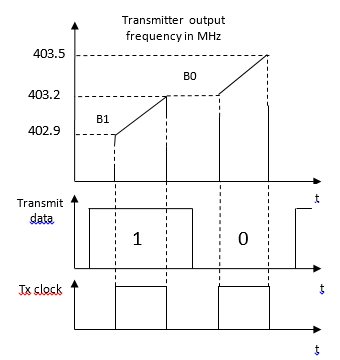 Figure 2. Output frequency of the transmitter in time domain
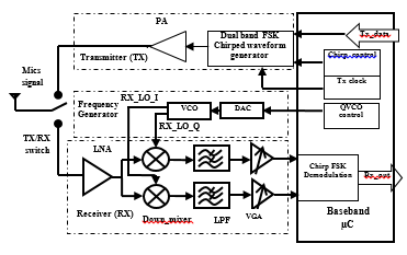 Figure 3. Illustration of zero-IF transceiver architecture.
Figure 3 shows different blocs of the proposed transceiver. The transmitter (TX) is composed of a dual band FSK chirped waveform generator and a power amplifier (PA).
A chirp control and Tx clock signals are used to switch between B0 and B1 signals depending on transmitted binary information and produces the LFM Binary FSK waveform. The power amplifier brings the signal power to the desired level in order to drive the antenna.
The RF band pass filter is not present in this design because it increases the noise figure and the circuit complexity of the receiver. In the other hand band pass filtering supplied by both antenna and LNA can mitigate the out-of-band signals at the receiver input.
After the antenna a LNA is used to amplify and band pass filter the received signal then the mixer down-converts it using quadrature LO signals. LO tones are produced with a VCO controlled by a Digital to Analog Converter (DAC). The DAC must generate the different voltages so that the VCO will be able to scan the entire RF frequency range from 402 MHz to 405 MHz with steps of 30 KHz. This technique is very useful for improving sensitivity and specially in presence of interferer. However, the system varies the LO frequency with a certain step to sweep the entire RF band and look for a clear channel and then perform the reception and demodulation. Before the VGA a low pass select filter (LPF) passes the desired channel and removes the other channels. Then a dual band chirped binary FSK demodulator based non coherent technique will recover the binary transmitted data [13].
3. Receiver design and simulation
In this work ADS tool is used for simulation and the receiver schematic is presented in figure 4. The aim of this simulation is to determine parameters for LNA, mixer, LPF and VGA that meet MICS and receiver specifications.
For this design the Pulse Rate Frequency (PRF) is set to 100 KHz and the bandwidth B is set to 300 KHz.
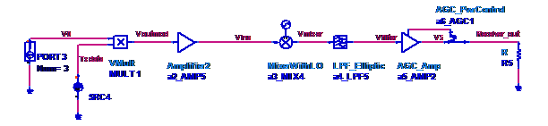 Figure 4. Receiver schematic.
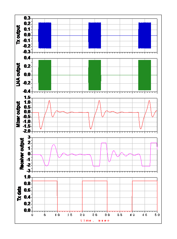 Figure 5. Tx binary data, Tx output, LNA output, mixer output and receiver output in time domain for =5ms, Pin = -16 dBm and a PRF of 100KHz
3.1. Spectrum at each node of the receiver
A harmonic balance simulation was made for both minimum and maximum receivers input power in order to evaluate receiver performances. Figure 5 presents time domain signals of the transmitted binary data (Tx data), transmitter output (Tx output) as spread spectrum BFSK signal, LNA output, mixer output and receiver output for =5ms, Pin = -16 dBm and a PRF of 100KHz.
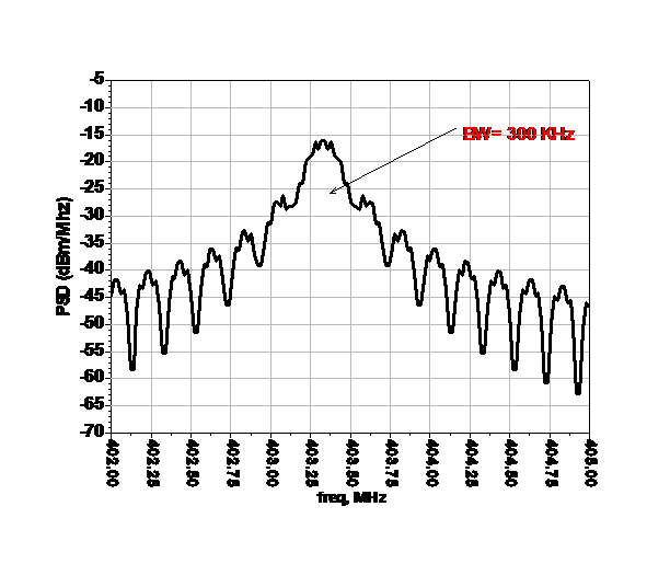 Figure 6. Receiver input in frequency domain
Figure 6 presents the spectrum at receiver input for channel number 5. We can see that the bandwidth B=300 KHz and the maximum input power Pin=-16 dBm. Figure 7 shows LNA output spectrum. Mixer output, LPF output and receiver output spectrums are shown in Figure 8 for maximum input power Pin=-16 dBm.
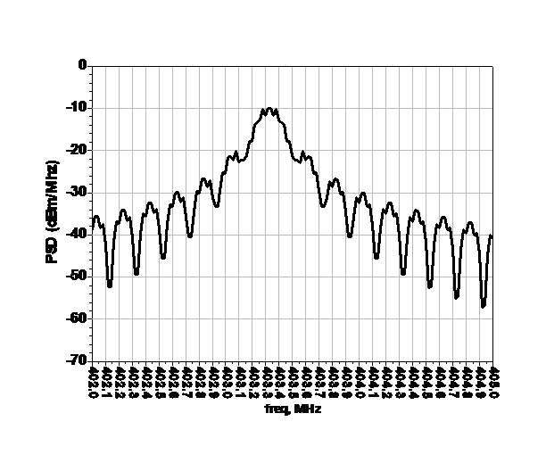 Figure 7. LNA output in frequency domain (Pin=-16 dBm)
It’s clear that the result of simulation of the output Power Spectral Density (PSD) aligns FCC mask requirements such as bandwidth 300 KHz. Therefore, the receiver down converts the received signal properly.
Figure 9 presents receiver input in frequency domain for input power Pin=-93 dBm which is the receiver sensitivity. In the same way, Mixer output, LPF output and receiver output spectrums are shown in Figures 10 and 11 for input power Pin=-93 dBm.
From Figures 7 and 11 we can notice that the receiver output dynamic range is between -62 dBm/MHz and 0 dBm/MHz. This power level can drive the chirped Binary FSK demodulator stage.
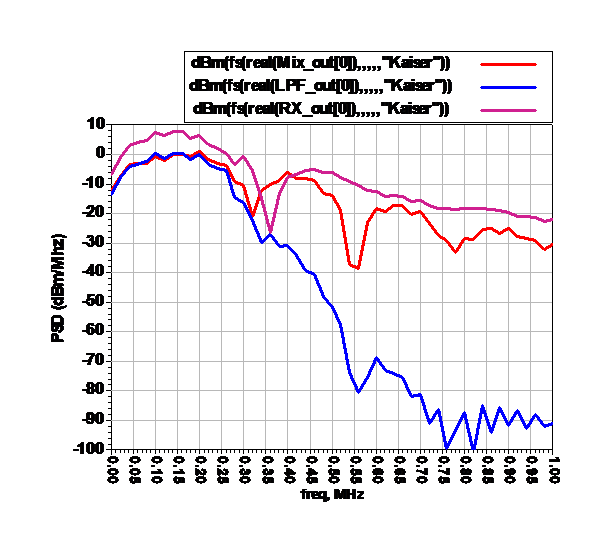 Figure 8. PSD for mixer, LPF and RX outputs, Pin=-16 dBm
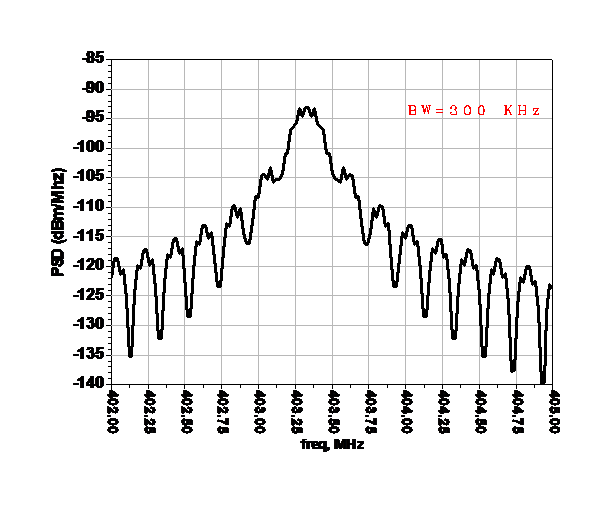 Figure 9. RX input in frequency domain for channel 5, Pin=-93 dBm
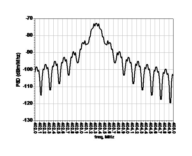 Figure 10. LNA output in frequency domain (Pin=-93 dBm)
3.2. LPF design
A variable bandwidth and sharp roll-off LPF has been used to select the clear channel from the 10 channels used in the MICS standard and reject at maximum interference. In this design we used a 5th order Elliptic filter with roll-off, 2dB rejection loss and 65dB attenuation. A tuning range from 40 KHz to 300 KHz is adopted as shown in figure 12. In addition this variable bandwidth Low Pass Filter can reject any narrowband interference by sweeping its bandwidth. This will improve the receiver performance.
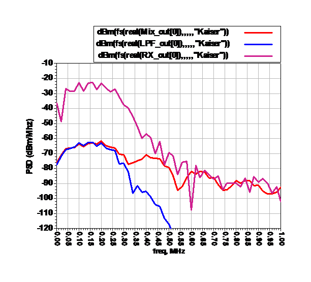 Figure 11. Spectrum for mixer, LPF and RX outputs, at a sensitivity Pin=-93 dBm.
3.3. Budget simulation
A Budget simulation for Pin= -16dBm was conducted which led to the following results: In Figure 13(a) the cascaded gain is 29dB, in Figure 13(b) the cascaded output power is equal to 13dBm and in Figure 13(c) the Noise Figure (NF) is 5.5dB.
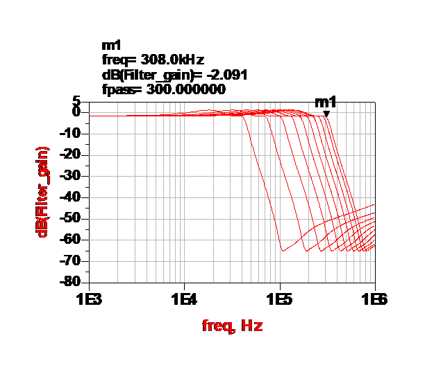 Figure 12. LPF response in frequency domain
For Pin= -93dBm (sensitivity) a Budget simulation was conducted which led to the following results: In Figure 14(a) the cascaded gain is 102dB, in Figure 14(b) the cascaded output power is equal to 10dBm and in Figure 14(c) the Noise Figure (NF) is 5.5dB.
Figure 13(d) demonstrates that the receiver achieves a P-1dB of -22.1dBm and an IIP3 of -12.6dBm. This means that the receiver is linear up to -22.1dBm. The sensitivity of the receiver (-93dBm) is an excellent value compared with Bluetooth or Zigbee communication systems. Therefore this receiver can detect strongly attenuated input signals. A receiver NF of 5.5dB is acceptable to achieve a bit error rate of 10-3.
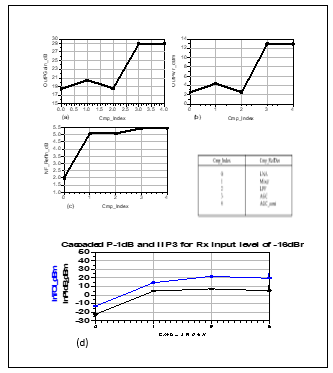 Figure 13. (a) receiver gain, (b) receiver output power, (c) receiver NF, (d) 1dB compression point and IIP3, for Pin=-16dBm.
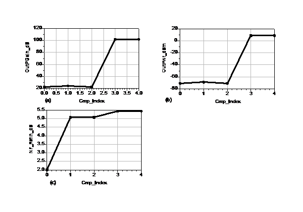 Figure 14. (a) receiver gain, (b) receiver output power, (c) receiver NF, for Pin=-93dBm.
4. FSK dual band Demodulator
The design of demodulator circuit for Binary Frequency Shift Keying (BFSK) modulation request simple circuits that consume low power. Non coherent demodulator based on an envelope detector, integrate and dump, a sampling and hold and a limiting circuit still provides acceptable performance for low complexity MICS receivers, especially in multipath environments.
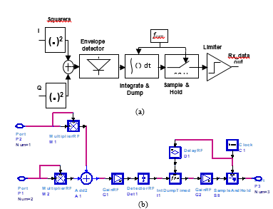 Figure 15. (a) block diagram of the Binary dual band FSK demodulator, (b) Implemented on ADS
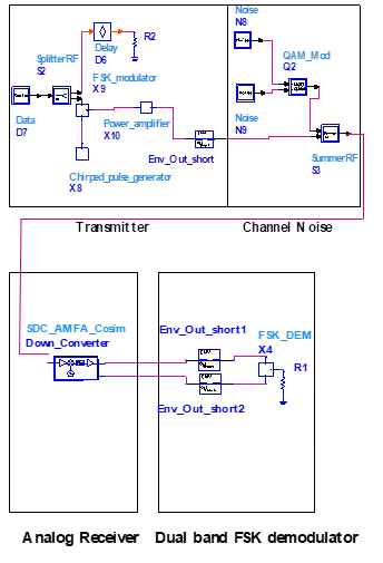 Figure 16. The template used to Co simulate the receiver with the chirped BFSK demodulator
Figure 15(a) presents the proposed FSK dual band demodulator. Advanced Design System tool was used to simulate this demodulator and the corresponding schematic is shown in Figure 15(b). Tow squarer (multiplier RF) are employed to perform energy detection. The I and Q signals are added (Add2). The combined signal is fed into an envelope detector then into integrate and dump block. After sampling-and-hold, a limiting amplifier will retrieve transmitted data. This technique provides acceptable performance for low complexity receivers, especially in multipath environment.
The analog transceiver with the chirped dual band FSK demodulator are co simulated and the corresponding template is shown in Figure 16. AWGN channel noise was used to run this co-simulation.
Figure 17 shows time representation of Tx data and chirped pulses for bit 1 and bit 0.
Figure 18 shows Tx spectrum for bit B1, bit B0 and the dual band Tx output spectrum. We can notice that the Tx output spectrum respects the FCC mask requirements for the MICS band. The emission power is under -16 dBm in order to avoid interferences with other communication services using the same MICS RF band.
The receiver output spectrum after low pass filtering and amplification is represented in Figure 19. The in band power of 0 dBm can drive the dual band FSK demodulator input.
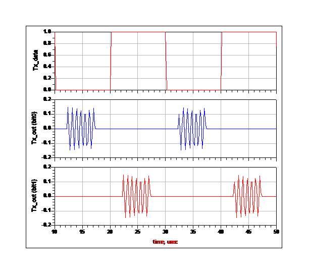 Figure 17. Time representation of Tx data and chirped pulses for bit 1 and bit 0
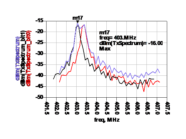 Figure 18. Tx spectrum for tp=5µs and PRF=100KHz
Figure 20 shows waveforms at the adder output (adder_out), on the output of the envelope detector (env_det_out), after the block of integration (int_out), at the sample and hold output (S&H_out) and at the system output (Rx_dataout).
The co-simulation results show that the binary signal at the output of the demodulator is exactly the same as the delayed binary signal transmitted. Thus proposed demodulator is working properly.
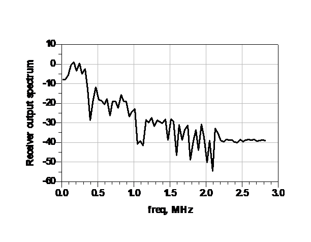 Figure 19. Output spectrum of the direct conversion receiver
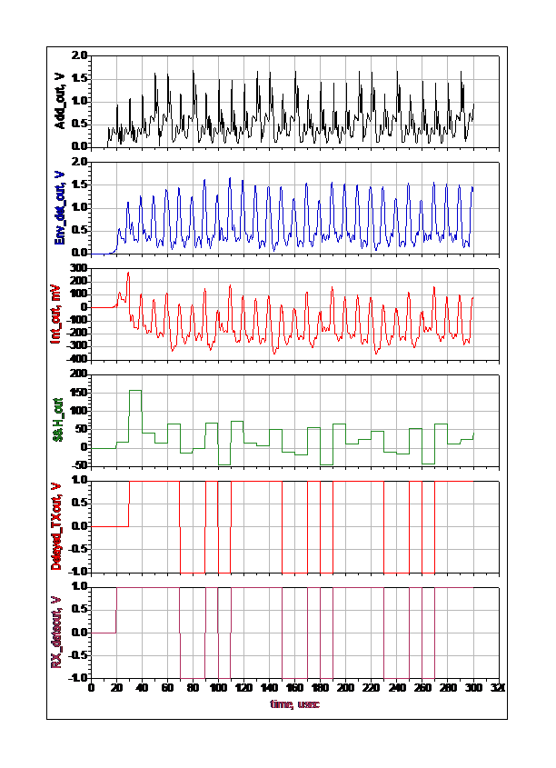 Figure 20. Time domain waveforms at different demodulator nodes
Table 1. Summary of the main technical parameters of the receiver
|
||||||||||||||||||||||||||||||||||||||||||
Table 2. Comparison with previously reported receiver
|
||||||||||||||||||||||||||||||||||||||||||||||||||||||||||||||||||||||||||||||||||||||||||||||||
5. Circuit blocks parameters and performance
The harmonic balance simulations results prove that the proposed design respects the constraints imposed by the FCC spectral mask and requirements of MICS standard.
In addition, the performance of the receiver is improved because it is able to reject any narrowband interference by sweeping the bandwidth of the LPF.
This chirped dual band BFSK demodulator can reply for the main challenge that is the low power. So, it is the best candidate for this kind of receiver. With this demodulator we can reach a better sensitivity.
In Table 1 we give a summary of the main technical parameters of the receiver showing its performance. The optimized specifications of the functions constituting the receiver are listed as well.
Table 2 shows a performance summary of the chirped BFSK MICS receiver. A comparison with other works dedicated for healthcare devices are listed as well.
It is proved that the proposed chirped BFSK MICS receiver designed using LFM technique and non-coherent dual band FSK demodulation has a sensitivity and a NF better than those found in the works [12], [14] and [16]. The results found in this design show that the proposed MICS receiver can be realized by simple, inexpensive and low consumption circuits which authorize healthcare implantable devices application.
6. Conclusion
A low-complexity LFM dual-band Binary FSK receiver for medical implantable wireless devices has been presented. A direct conversion architecture without RF band pass filter was used to avoid image interference and reduce circuit complexity. Linear Frequency Modulation technique was used to generate chirped Binary FSK signals. In order to reach low power implementation a simple non coherent demodulator was adopted. It is based on an envelope detector and simple decision circuits. Time domain, frequency domain and budget simulations results has been presented. We demonstrate that the proposed design respects the constraints imposed by the FCC and MICS requirements. A co-simulation of the analog receiver with the proposed non coherent demodulator shows that the receiver can reach a sensitivity of -93 dBm. In addition, the receiver is robust because it is able to reject any narrowband interference by sweeping the bandwidth of the LPF. This design allows the total integration of the sensor node in the same chip using low power CMOS technology. It promotes its use on a large scale in sensor networks implanted in the human body. This will essentially help people with disabilities, people with chronic diseases, people living alone and aged people to overcome their disabilities and live like healthy people.
Conflict of Interest
The authors declare no conflict of interest.
- M. Bettaieb, H. Trabelsi and M. Masmoudi, “A Novel MICS Chirp FSK Receiver Front-End” in International Conference on Engineering & MIS ICEMIS2017, Monastir, Tunisia, May 2017.
- Voskerician G., Shive M.S., Shawgo R.S., Von Recum H., Anderson J.M., Cima M.J., Langer R. “Biocompatibility and biofouling of MEMS drug delivery devices” Biomaterials, 24(11), 2003, pp.1959-1967.
- World Population Ageing 2015, Departement of economic and social affairs Population Division.United States.New York, 2015.
- H.S. Savci,A. Sula,E. Arvas, “MICS Tranceivers: Regulatory standard and applications”, in Proc.of Southest Con,April 2005, pp. 179-182.
- J. Ryckaert, M. Badaroglu, V. D. Heyn, G. V. der Plas, P. Nuzzo, A. Baschirotto, S. D’Amico, C. Desset, H. Suys, M. Libois, B. V. Poucke, P. Wambacq, and B. Gyselinckx, “A 16 mA UWB 3-to-5 GHz 20 M pulses/s quadrature analog correlation receiver in 0.18 µm CMOS,” in IEEE ISSCC Dig. Tech. Papers, pp. 368–377, 2006.
- FCC Rules and Regulations, “MICS Band Plan” , Part 95, jan 2003.
- D. C. Daly and A. P. Chandrakasan, “An energy efficient OOK transceiver for wireless sensor networks,” IEEE J. Solid State Circuits, vol. 42, no. 5, pp. 1003–1011, 2007.
- J. Ayers, N. Panitantum, K.Mayaram, and T. S. Fiez, “A 2.4 GHz wireless transceiver with 0.95 nJ/b link energy for multi-hop battery free wireless sensor networks,” in Symp. VLSI Circuits Dig. Tech. Papers, pp. 29–30, 2010.
- H. Trabelsi, Gh. Bouzid, F. Derbel and M. Masmoudi, “A 863-870MHz Spread Spectrum FSK Transceiver Design for Wireless Sensor,” Microelectronics Journal (MEJ), vol. 41, No 8, pp 465-473, August 2010.
- Simanjuntak, Lastri, “A Novel Chirp Slope Keying Modulation Scheme for Underwater Communication”, University of New Orleans Theses and Dissertations. Paper 201, December 2004.
- R. Roovers, D. M. W. Leenaerts, J. Bergervoet, K. S. Harish, R. C. H. van de Beek, G. van der Weide, H. Waite, Y. Zhang, S. Aggarwal, and C. Razzell, “An interference-robust receiver for ultra-wideband radio in SiGe BiCMOS technology,” IEEE J. Solid-State Circuits, vol. 40, pp. 2563–2572, 2005.
- BA et al, “ a 0.33nJ/bit IEEE802.15.6/Proprietary MICS/ISM Wireless Transceiver With Scalable Data Rate for Medical Implantable Applications”, IEEE Journal of Biomedical and Health Informatics, Vol.19 .No.3, May 2015.
- H. Trabelsi, I. Barraj and M. Masmoudi “A 3-5 GHz FSK-UWB Transmitter For Wireless Personal Healthcare Applications”; International Journal of Electronics and Communications (IJEC), Vol. 69, pp. 262-273, 2015, DOI:10.1016/j.aeue.2014.09.009.
- P. D. Bradley, “An Ultra-Low power, high performance medical implant communication system (MICS) transceiver for implantable devices,” in Proc. IEEE Biomed. Circuit Syst. Conf., pp .158-161, December 2006.
- V. Peiris, C. Arm, S. Bories, S. Cverveny, F. Giroud, P.Graber, S. Gyger, E. Le Roux, T. Melly, M. Moser, O. Nys, F. Pengg, P.-D. Pfister, N. Raemy, A. Ribordy, P.-F.Ruedi, D. Ruffieux, L. Sumanen, S. Todeschin, and P. Volet, “ A 1V 433/868MHz 25kbps-FSK 2kbps-OOK RF transceiver SoC in standard digital 0.18μm CMOS,” in Proc. IEEE Int. Solid-State Circuits Conf. Dig. Tech. Papers, pp. 258-259, February 2005.
- S. Kim, W. Lepkowski, S. J. Wilk, T. J. Thornton and B. Bakkaloglu, “A Low-power CMOS BFSK Transceiver for Health Monitoring Systems” in IEEE Biomed Circuits Syst Conf. 2011, 157–160. doi:10.1109/BioCAS.2011.6107751.
No related articles were found.