On The Development of a Reliable Gate Stack for Future Technology Nodes Based on III-V Materials
 , Sonja Sioncke 1, Jacopo Franco 1, Vamsi Putcha 1, 2, Laura Nyns 1, Arturo Sibaja-Hernandez 1, Rita Rooyackers 1, Sergio Calderon Ardila 2, Valentina Spampinato 1, Alexis Franquet 1, Jan Maes 3, Qi Xie 3, Michael Givens 4, Fu Tang 4, Xiang Jiang 4, Marc Heyns 1, 2, Dimitri Linten 1, Jerome Mitard 1, Aaron Thean 5, Dan Mocuta 1, Nadine Collaert 1
Adv. Sci. Technol. Eng. Syst. J. 3(5), 36–44 (2018);
 DOI: 10.25046/aj030506
In this work, we discuss how the insertion of a LaSiOx layer in between an in-house IL passivation layer and the high-k has moved the III-V gate stack into the target window for future technology nodes. The insertion of this LaSiOx layer in the gate stack has reduced the Dit and Nbt below the target level of 5×10¹¹ /eV.cm2 and 3×10¹⁰ /cm2 (target at 10 years operation: Vfb<30mV at 125°C) respectively. From physical analysis, it was found that LaSiOx can stabilize the interaction of the IL layer with the InGaAs substrate. An implant free In0.53Ga0.47As n-MOSFET was fabricated with this gate stack and for the first time, a III-V gate stack meets the reliability target for advanced technology nodes with a max operating Vov of 0.6 V. In addition, an excellent electron mobility (µeff,peak=3531 cm2/V-s), low SSlin=71 mV/dec and an EOT of 1.15 nm were obtained. We also report the scaling potential of this stack to 1 nm EOT without any loss in performance, reliability and further reduction of the sub-threshold swing (SSlin=68 mV/dec).
1. Introduction
III-V compound semiconductors have already been widely investigated as an alternative material to Silicon for future Metal -Oxide-Semiconductor Field Effect Transistors (MOS-FETs). MOS devices based on III-V compound semiconductor materials like InGaAs, with excellent performance, have been demonstrated on both 2-inch InP substrates and on a 300mm Si platform [1-5]. But, in order to become a commercially viable alternative to existing Si technologies, two major issues are yet to be solved: 1) the defective interface between III-V materials and the high-k oxide layers, and 2) the high density of defects in the most commonly investigated high-k oxides, Al2O3 and HfO2.
Both of these issues have been shown to affect almost every aspect of device performance, such as the capacitance [6-11], reliability of III-V based devices [11-14], on-state electrical parameters like mobility [15], and trans-conductance [16, 17]. As a result, it becomes extremely important to reduce their impact in order to make commercial III-V MOSFET technology a reality. In this regard, the use of a new IL layer in combination with an Al2O3/HfO2 or just HfO2 stack was reported, showing improved performance and a significant reduction of the oxide traps. However, with the requirement of a thin Al2O3 layer for gate stack thermal stability and due to the wide defect distribution in Al2O3, the total density of charging oxide traps was still higher than the target (10 years reliability target: flat-band voltage shift, ΔVfb < 30 mV at 125°C. Assuming a typical time power law exponent of 0.13, the failure criterion projects effective density of charged defects, ΔNeff to < 3×10¹⁰/cm2 at operating field, for an Effective Oxide Thickness (EOT) of 1 nm [18, 19]).
This paper is an extension of the work presented in IEEE Symposium on VLSI Technology 2017. In this paper, we demonstrate and comprehensively discuss on the process of replacing Al2O3 in the IL/Al2O3/HfO2 gate stack with LaSiOx. Furthermore, we elaborate on the improvements, thereof, in the interface properties and reliability for operation at VDD=0.8 V, which exceeds the operating target for future technology nodes without any loss in the electrical performance of the MOSFET device reported earlier.
2. Experimental details
Capacitors were made starting from an MBE grown 300 nm n-type In0.53Ga0.47As on 2-inch n-type InP substrates. The targeted Si doping in the In0.53Ga0.47As grown layer was ~1×10¹⁷ at/cm3. Prior to the gate stack deposition, the substrates were cleaned in a 2M HCl solution for 5 min at room temperature and subsequently rinsed in de-ionized water. H2S pretreatment and deposition of the IL (Inter Layer), LaSiOx, Al2O3 and HfO2 were done in an ASM Pulsar® 3000 ALD reactor. The H2S pretreatment is done in-situ prior to the high-κ deposition. The IL used here is an ALD based layer with a κ-value ~6. The H2S treatment and IL film deposition are both done at 250°C. Al2O3 and HfO2 were deposited by ALD TMA/H2O and HfCl4/H2O at 300°C. LaSiOx is deposited by an ALD process at 250°C using the following precursors: LoLaPrime® (AIR Liquide), SiCl4, H2O. A 42% La concentration in the LaSiOx is obtained by using a La:Si pulse ratio of 1:5. A full ALD cycle consists of : [[SiCl4/purge/H2O/purge] x 5 + [LolaPrime/purge/H2O/purge] x 1] x n. Under these conditions, a GPC of 0.1754 nm is achieved.
Dot capacitors were fabricated by sputtering 80 nm TiN using physical vapor deposition (PVD). A dry-etch process was used to etch the metal gate. An anneal in forming gas (10% H2/N2) was done prior to metal deposition (PDA) or post metal deposition (PMA) at 400°C for 5 min.
Implant-free quantum-well devices were also fabricated to study the impact of these passivation schemes on the device performance and reliability. A schematic diagram of the quantum-well MOSFET is shown in Fig.1. The stack for MOSFETs consists of a 15 nm un-intentionally doped In0.53Ga0.47As channel layer, a 3 nm InP etch stop layer and a 50 nm n+ In0.53Ga0.47As (Si-doped, 1×1019 cm-3) layer, all grown on a 2-inch semi-insulating InP substrate. Fig. 2 describes the process flow used in this work. The detailed device fabrication can be found in [20]. Prior to gate stack deposition, a digital etch (cycles of HCl and H2O2) was used to clean and smoothen the InGaAs channel surface. The different gate stacks that were studied are depicted in Table I.
I-V and C-V measurements were used to study the impact of the gate stack on the performance of the devices. I-V measurements were carried out using HP4156 parameter analyzer and C-V measurements were performed using a HP4284A-LCR meter. The interface defect density, Dit, is extracted using the conductance method from the parallel equivalent conductance Gp [21] at room temperature. The amount of oxide traps (ΔNeff) are measured by C-V hysteresis measurements (forward and reverse sweep of the gate voltage) at different maximum stress voltages and the corresponding shift in flat band voltage, ΔVfb, measured between the forward and backward trace is converted into a sheet charge (ΔNeff (Eox)). The flat-band voltage is the gate voltage corresponding to an inflection point in the double derivative of the normalized capacitance-voltage data at a frequency of 100 kHz [21,22]. The ΔNeff at target field as well as the voltage acceleration
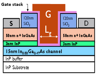 Figure. 1. Schematic representation of the MOSFET device (Dimensions are not to scale).
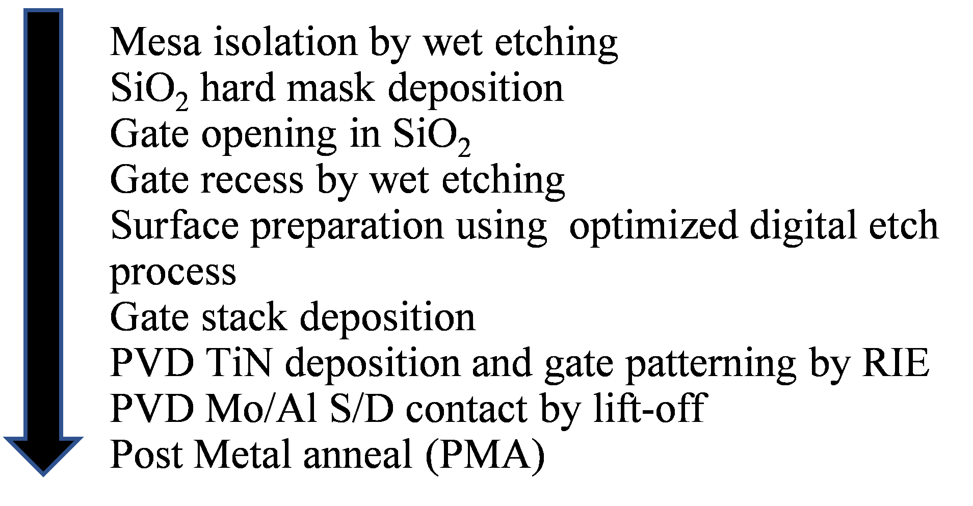 Figure 2. Process flow used in this work for MOSFET fabrication.
Table 1: Split table of III-V gate stacks
|
factor (γ, i.e. the slope of the log-log plot of ΔNeff vs Eox) is reported as a figure of merit to study the oxide trap behavior [23]. Although this method does not take into account the influence of stress temperature and stress time into account, it helps in identifying the trends between different gate stack/pretreatments. Bias temperature instability (BTI) characterization using extended Measure-Stress-Measure (eMSM) technique was used to evaluate the reliability of the MOSFET devices [23]. Finally, Time-Of-Flight Secondary Ion Mass Spectrometry (TOFSIMS) was used to study the chemistry of the stacks.
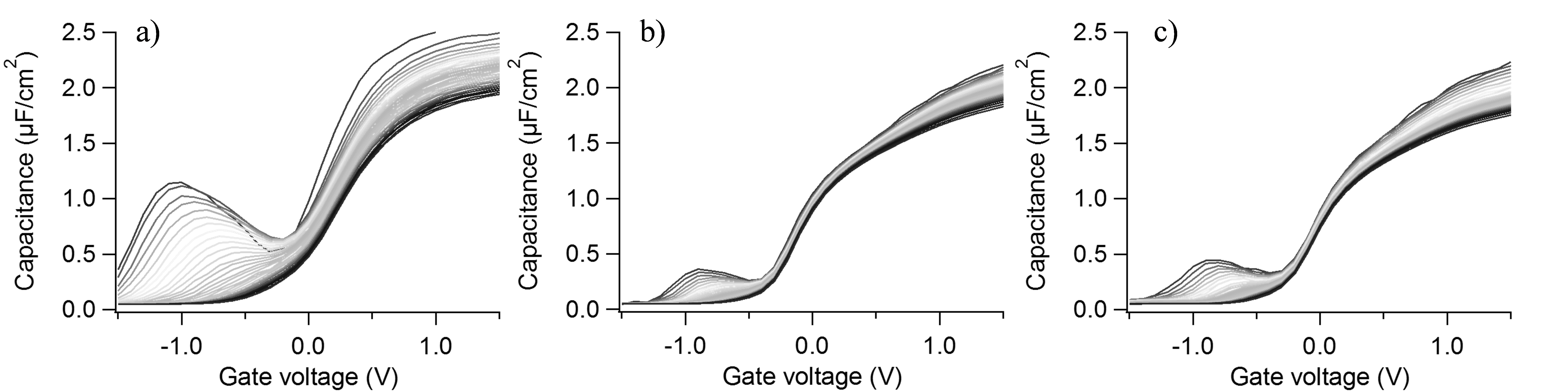 Figure 3. Measured RT CV’s of gate stacks a) ‘ref’, b) A and c) B’ described in Table I at 31 frequencies between 1kHz and 1MHz. The MOSCAP devices received a PDA at 400°C, 5’ in Forming gas.
3. Results and discussion
3.1. The IL layer development and thermal stability
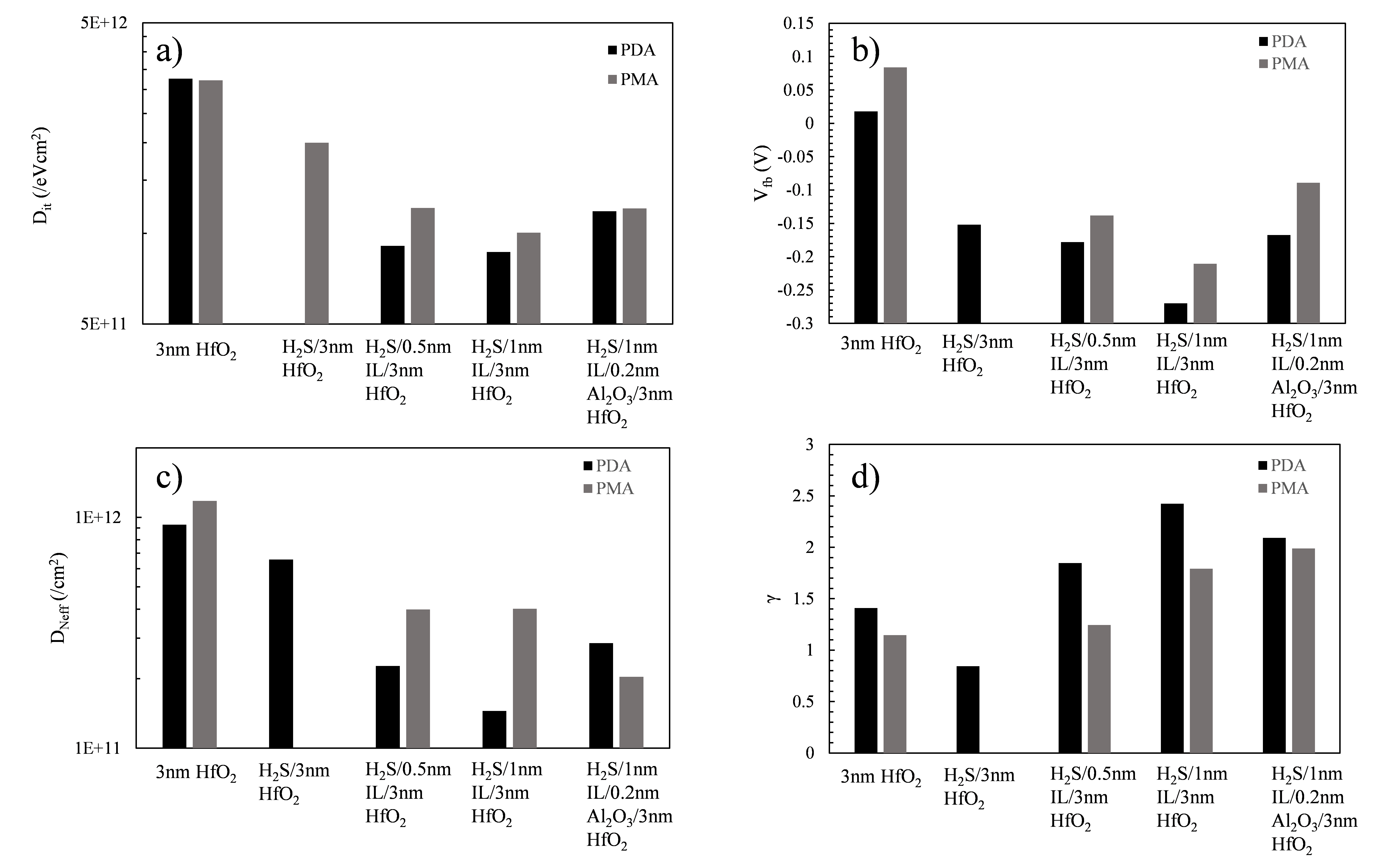 Figure 4. Electrical parameters extracted for gate stacks ‘ref’, A, A‘, B’ described in Table I. a) Midgap Dit extracted from RT CV’s. b) Vfb c) ΔNeff extracted from RT CV hysteresis by converting the measured ΔVfb into an effective charge sheet at the interface by: ΔNeff=ΔVfb*Cox/q, and reported at charging equivalent field of 3.5 MV/cm [13]. Vstart condition was taken at Vg=-1.5V. d) Field acceleration exponent, γ, i.e. the slope of the log-log plot ΔNeff vs oxide field which is a measure of the misalignment between the channel carrier energy-i.e. InGaAs Ef– and defect levels in the high-k. Filled bars represent the data after PDA, shaded bars represent the data after PMA.
Fig. 3 shows the multi-frequency (1 kHz – 1 MHz) C-V for various samples in the split table of Table I, measured at room temperature. The reduction in the Dit bump and in frequency dispersion when inserting the IL (3-A,B’) between the InGaAs channel and the HfO2 layer clearly shows the improvement. Fig. 4 shows the result of the extraction of various electrical parameters from the measured C-V data. The extracted mid-gap Dit drops by more than a factor of 2 when inserting the IL accompanied with a negative flat band voltage, Vfb, shift (Fig. 4a,b). An H2S treatment prior to the HfO2 deposition has a similar effect: it reduces the Dit and shifts the Vfb by -0.15 V. Compared to an H2S treatment, the insertion of 1 nm of the IL layer shifts the Vfb to even more negative values and a larger reduction in Dit is observed. In addition, the IL layer reduces the ΔNeff by 1 order of magnitude and increases the γ-value to 2.5. Although 0.5 nm of the IL layer shows similar trends, an optimum is reached when using 1nm of the IL layer. This result suggests that 1 nm of IL is needed to form a closed layer passivating the interface. When adding a thin (0.2 nm) Al2O3 cap on top of the IL layer, the Dit bump and frequency dispersion increase slightly (Fig. 3-B’). One can also observe that the Vfb shifts to more positive values and this goes hand in hand with a slight increase in ΔNeff and reduction of the γ value. From these observations, a hypothesis can be put forward. Fig. 5 depicts
 Figure 5. Defect band model to explain the observed changes in the γ value and total amount of charged oxide traps at a given field. The IL passivation layer is creating a dipole shifting the misalignment between InGaAs Ef and defect levels in the high-κ. In Al2O3 a partial overlap between deep and shallow traps is existing [9] and an almost uniform defect band is present. Therefore, the dipole created is not as effective as compared to the situation where deep and shallow traps are well separated as is proposed for the stack with HfO2.
a cartoon of a possible explanation. Defect band modeling [24,25] has shown that although peak defect densities in Al2O3 are lower, a partial overlap of the defect bands induces an almost uniform distribution of defect levels around the InGaAs conduction band edge, Ec. On the contrary, HfO2 on InGaAs shows a minimum defect density slightly below the channel Ec (~0.2 eV below Ec), which can be exploited for improving gate stack reliability by introducing an interface dipole. The assumption is that the IL layer gives rise to such a dipole shifting the defect levels up with respect to the InGaAs Ec and shifting the minimum level into the device operating range. However, dipole engineering is not effective when a broad defect band without a clear minimum is present as is the case with Al2O3.
From the results shown till now, one can conclude that the 1 nm IL/3 nm HfO2 stack shows an optimum for all electrical parameters although the Dit and Nbt levels are still above the targeted values (5 x 10¹¹ /eV.cm2 and 3 x 10¹⁰ /cm2 respectively). However, when applying a PMA, we observe that the 1 nm IL/3 nm HfO2 stacks degrades slightly i.e. a Dit, ΔNeff increase and a reduction in the gamma value is observed in combination with a positive Vfb shift (Fig. 4-shaded bars). On the contrary, the stack with the Al2O3 cap does not degrade when a PMA is added. This result implies that although the initial gate stack properties are degraded when adding an Al2O3 cap, this cap can help in stabilizing the gate stack upon a PMA.
 Figure 6. RT MF-CV’s measured from dot capacitors of A) 1 nm IL/3 nm HfO2, B) 1 nm IL/1 nm Al2O3/3 nm HfO2, C) 1 nm IL/1 nm LaSiOx/3 nm HfO2, C’) 1 nm LaSiOx/3 nm HfO2. Frequencies between 1 kHz-1 MHz (red-blue) were measured with logarithmic spacing. All capacitors received a PMA in forming gas for 5 minutes.
In conclusion, the IL approach provides an improved interface quality and increases the misalignment between the InGaAs channel Ef and the defect bands in the high-κ. The improved interface quality was proven to increase the performance of InGaAs MOS devices on both planar as well as nanowire architectures. However, the introduction of a cap layer is needed to provide a good thermal stability. Although Al2O3 can provide a higher stability for thermal processing, the unfavorable defect band distribution in the Al2O3 does not allow for dipole engineering. In the next part, we show that a LaSiOx cap can provide both an improved thermal stability and a more favorable defect band distribution.
3.2. Replacement of Al2O3 stabilization cap by LaSiOx
Fig. 6 shows the multi-frequency C-V for various gate stacks in Table I and demonstrates the impact of the insertion of LaSiOx between the IL passivation and HfO2. All the dot capacitors were measured after PMA at 400oC in forming gas anneal for 5 minutes. Although the CV’s from the 1 nm IL/3 nm HfO2 stack (Fig. 6A) and the 1 nm IL/1 nm LaSiOx/3 nm HfO2 stack (Fig. 6C) look similar, one can notice that the frequency dispersion is further reduced when LaSiOx is inserted between the IL and HfO2. As was discussed in the previous section, an Al2O3 cap degrades the gate stack properties slightly. Although the difference between the stacks with the IL are subtle, a large difference can be observed when the IL is removed (Fig. 6C’). These results imply that both the IL and the LaSiOx cap are needed to optimize the gate stack properties.
The Dit, extracted at mid gap, and capacitance equivalent thickness (CET) are shown in fig. 7. The insertion of the IL (A) reduces the mid gap Dit as was already reported in the previous section. The replacement of Al2O3 (B) by LaSiOx (C) further reduces the Dit and a reduction of the CET is also observed (CET=1.55 nm, EOT=1.15 nm). In addition, the total density of charging oxide traps drops to a value close to 1 x 10¹⁰ /cm2 at Eox
 Figure 7: Mid gap Dit (bars) and CET (dots) extracted from the C-V data presented in fig. 6. Replacement of Al2O3 (B) by LaSiOx (C) reduces the Dit to less than 4 x 10¹¹ /cm2eV. The CET drops to 1.55 nm.
 Figure 8: ΔNeff (bars, left axis) extracted from C-V hysteresis (Vstart=Vfb – 0.5 V) by converting the measured ΔVfb into an effective charge sheet at the interface by: ΔNeff=ΔVfb*Cox/q, and reported at charging equivalent field of 3.5 MV/cm [6]. Field acceleration exponent, γ, (dots, right axis) i.e. the slope of the log-log plot ΔNeff vs oxide field which is a measure of the misalignment between channel carrier energy-i.e. InGaAs Ef and defect levels in the high-k [18].
= 3.5 MV/cm (Fig. 8) meeting the target for 10 years operation (10 years reliability criterion: ΔVfb < 30 mV at 125°C. Assuming a typical time power law exponent of 0.13, the failure criterion projects ΔNeff to less than 3 x 10¹⁰ /cm2 at operating field, for an EOT of 1 nm). The reduction of oxide traps below the target level is the result of the combination of the IL layer and LaSiOx cap: while the IL layer increases the field dependence of the ΔNeff (γ ~ 3.5), which is beneficial only for low voltage operation, the LaSiOx cap consistently reduces the density of charging defects irrespective of the operating voltage.
 Figure 9. 100 kHz CV up and down traces of the 1 nm IL/1 nm LaSiOx/3 nm HfO2 gate stack measured at 3 different Vmax. Vstart was Vfb-0.5V.
Fig. 9 shows the forward and backward sweep of gate voltage for the C-V hysteresis measured at different Vmax for 1 nm IL/1 nm LaSiOx/3 nm HfO2 stack. At low overdrive voltages, the hysteresis is negligible. Only at higher overdrive voltages, a clear hysteresis can be measured. Notice also that the starting voltage for these measurements was carefully chosen at Vfb – 0.5 V. As was reported in [25], the C-V hysteresis measurements can largely depend on the Vstart condition, as is also the case for gate stack under evaluation (Fig. 10). The more negative Vstart condition reflects the discharging of deep traps that can take place during OFF-state, when the device is biased deep into the depletion and is an equally important criterion to take into account. Measuring at Vstart=Vfb – 0.5 V shows that oxide trap densities are within target. Starting from a more negative Vg, the oxide trap density increases and γ decreases. This observation indicates that this gate stack has a low
 Figure 10: ΔNeff as a function of applied Eox for the stack with 1 nm IL/1 nm LaSiOx/3 nm HfO2 for 2 different Vstart conditions. Vstart=-1.5V and Vstart=Vfb-0.5V. The large dependence on the Vstart conditions points to the presence of deep traps i.e. located at energies below InGaAs Ef at flatband.
amount of electron traps, but a more negative Vstart charges hole traps, thereby increasing the total amount of traps during the measurement and decreasing the voltage dependence.
Therefore, BTI measurements were performed at both positive and negative stress conditions to capture the max Vov for both stress conditions (Fig. 11). From these CV-BTI measurements, one can see that the 1 nm IL/1 nm LaSiOx/3 nm HfO2 stack meets the
 Figure 11: Max Vov measured from positive and negative CV-BTI on MOS capacitors. For a target VDD=0.8V, the max pos Vov target (full line) is 0.53V and the max neg Vov target (dashed line) is -0.26V (i.e. 1/3*VDD).
 Figure 12. TOFSIMS positive ion profiles from MOSCAPs of stacks a) A, b) B and c) C from Table I. All layers are aligned at the peak of the IL atom profile. max Vov target (for a VDD=0.8 V) for both stress conditions. When removing the IL layer, none of the targets are met. As III-V materials will be introduced in technologies operating at VDD=0.5V and resulting target Vov=0.33 V (=2/3*VDD), this implies that these MOSCAP In0.53Ga0.47As devices with the 1 nm IL/1 nm LaSiOx/3 nm HfO2 gate stack surpass the IIIV reliability requirements.
Stabilization of the IL by the Al2O3 or LaSiOx cap is confirmed from the TOFSIMS profiles measured on dot capacitors that received a PMA (Fig. 12). These profiles show the mixing of the Al atoms (from the Al2O3) or La atoms (from the LaSiOx) with the IL. Diffusion of the IL atoms down into the InGaAs substrate is clearly present if no cap layer is deposited between IL and the HfO2 (Fig. 12a). When an Al2O3 or LaSiOx cap is added on top of the IL (Figs. 12b and 12c) , a steep slope of the IL elements down into the substrate is observed. The hypothesis is that the mixing of the Al or La atoms with the IL atoms is increasing the stability of the IL. Although the chemistry from both Al2O3 and LaSiOx cap layers can provide stabilization of the interaction of the IL with the substrate, the electrical characteristics of the LaSiOx cap are more favorable.
Modeling of the shallow and deep defect bands using the approach as described in [26], was done and explains the effect of the LaSiOx cap (Fig. 13). The introduction of the IL layer narrows the distribution of the shallow defect band as well as shifts the mean energy of that band to shallower energies. Adding LaSiOx in between the IL and HfO2 further reduces the charging defect density. This reduction can be attributed to the stabilization that is provided by the LaSiOx cap.
3.3. MOSFET device characteristics
Figs. 14 and 15 show the Ids-Vgs and gm-Vgs curves of the devices fabricated with stacks B (Al2O3 cap) and C (LaSiOx cap). Excellent device characteristics in the form of high Ion/Ioff ratio (> 2×10⁶, > 8×10⁵ at Vds=0.05 V and 0.5 V respectively) and low SSlin (< 75 mV/dec) were extracted for both the gate stacks. The device characteristics for stacks B, C, C’, and C’’ are given in Fig. 16 and 17. The on-state current increases (Fig. 16a and b) and the SSlin decreases (Fig. 17) when Al2O3 (B) is replaced by LaSiOx (C) between the IL layer and HfO2. When scaling the HfO2 to 2 nm (C’’), a CET of 1.46 nm (EOT of 1.06 nm) is achieved with a
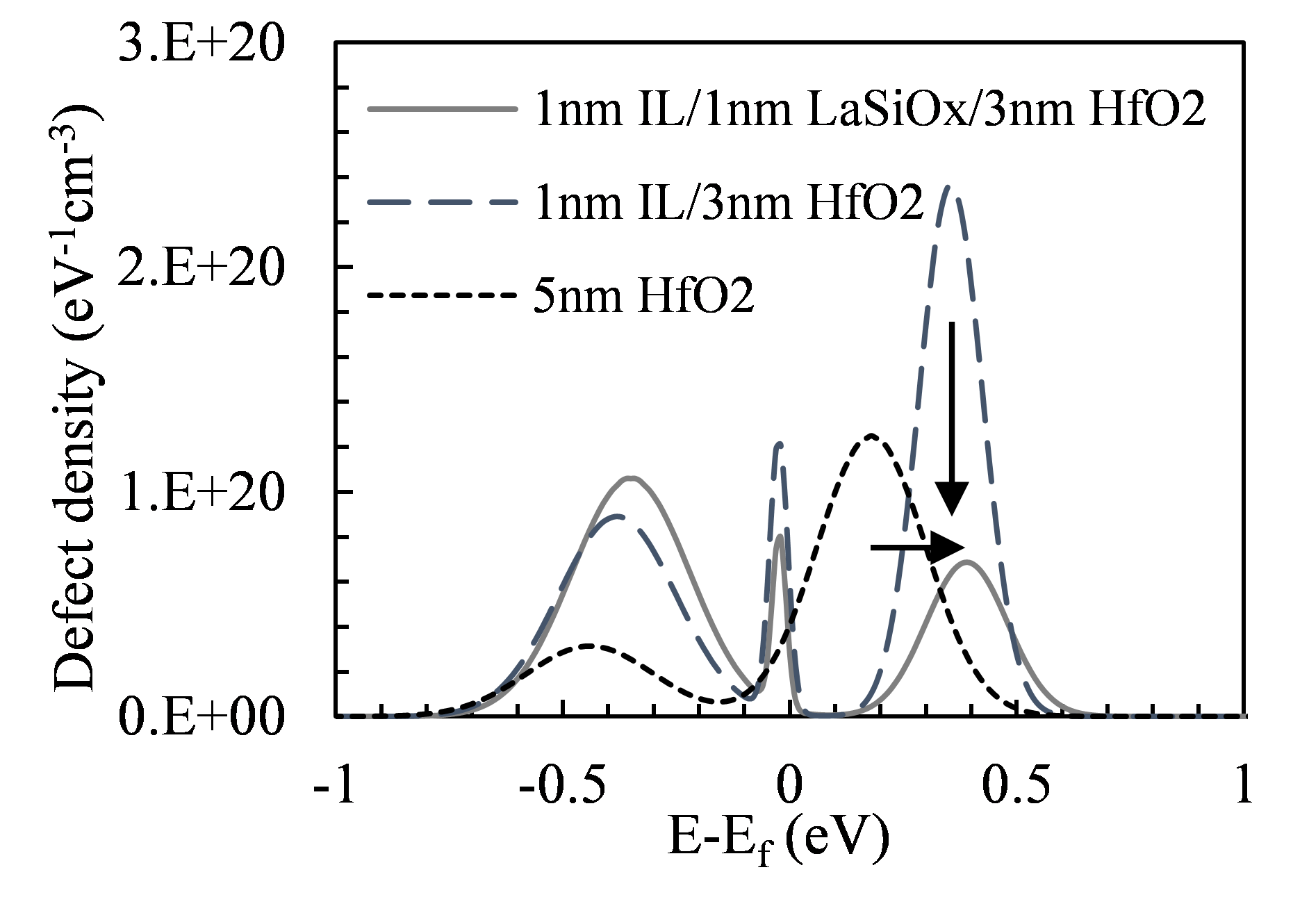 Figure 13: Defect density profile obtained by modeling the ΔVth vs Vgate as described in [25]. Insertion of the IL layer causes narrowing of the shallow defect band, thus enhancing γ and shifting the mean defect level of this band to shallower energy [19] but increases the density of defects at deeper energies. Insertion of LaSiOx consistently reduces the total defect density (both shallow and deep energies). further improvement in the on-characteristics, and with a reduction in the SSlin to 68 mV/dec. Note that the stack without the IL layer (1 nm LaSiOx/3 nm HfO2 stack only, C’), exhibits high on-current compared to the stack with the 1 nm IL/1 nm Al2O3/3 nm HfO2 but
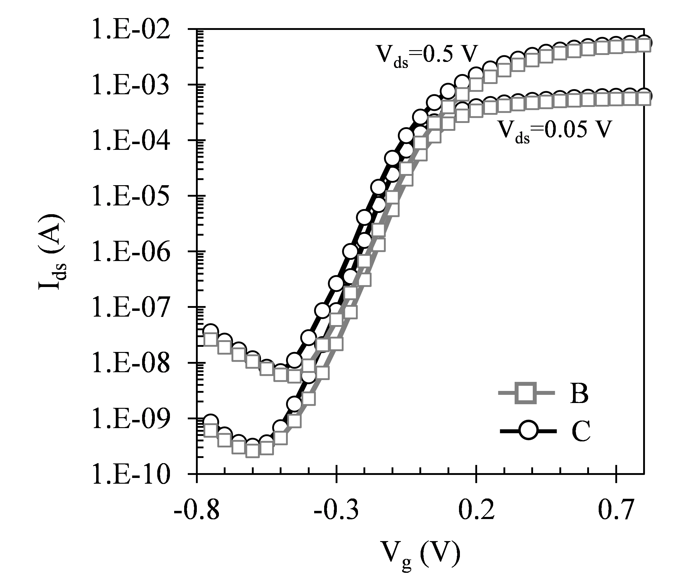 Figure 14: Ids-Vgs for Lg=10 µm, W=100 µm device.
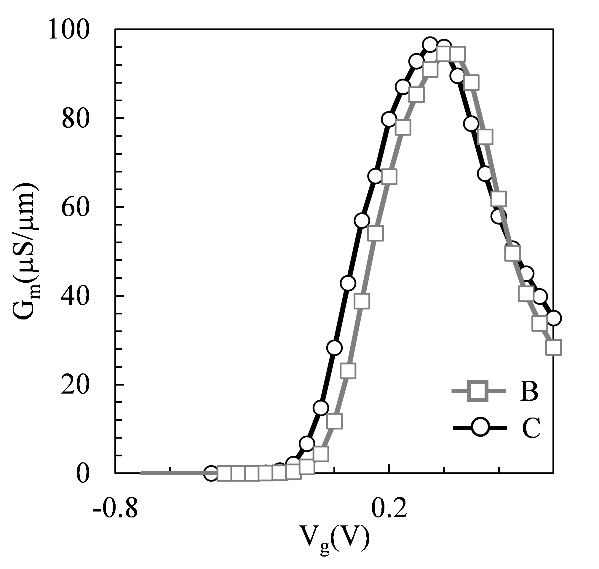 Figure 15: Gm-Vgs for Lg=10µm, W=100µm device.
 Figure 16: Ion extracted at Vt+0.5V and for Vds=0.05V (a) and Vds=0.5V (b), W of the devices = 100µm, Lg=10µm. Replacement of Al2O3 (B) by LaSiOx (C) in the gate stack improves Ion. Further improvement can be seen when the gate stack is scaled down (C’’).
also a high SSlin reflecting a higher mid gap Dit extracted from the MOS capacitor C-V’s (Fig. 7 and 8). Only slight changes in Vth_lin (~50 mV) are observed when changing the stabilization cap (Fig. 18).
The mobility data (Fig. 19) reveal that while the dominant
 Fig. 17 SSlin for various gate stacks. Lg=50 µm. SSlin reduces by replacing Al2O3 (B) with LaSiOx (C) in the gate stack. Scaling the HfO2 (C’’) thickness leads to further reduction.
 Figure 18 Vt, lin for various gate stacks. Lg=50 µm. Slight Vtlin reduction by replacing Al2O3 (B) with LaSiOx (C) in the gate stack is observed.
impact of insertion of the IL layer is on the peak mobility (µeff at peak = 3531 cm2/V.s), the replacement of the Al2O3 by LaSiOx increases the electron mobility at high charge carrier density.
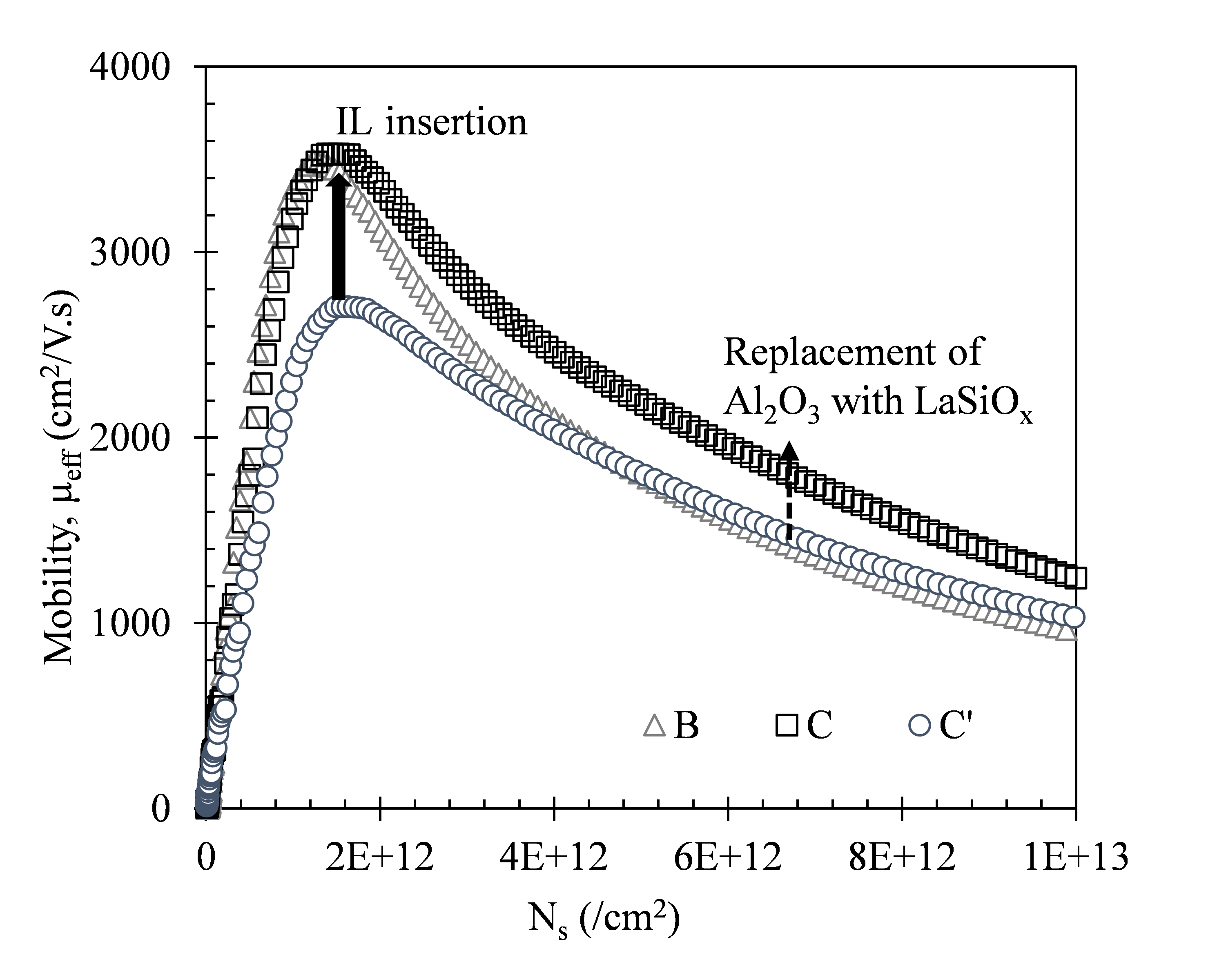 Figure 19 Improvement in the mobility at low Ns (due to the introduction of IL) and high Ns (as a result of replacement of Al2O3 with LaSiOx). Mobility was extracted from Lg=50 µm devices.
This observation suggests a reduction in the roughness using LaSiOx in the gate stack instead of Al2O3. In addition, BTI measurements on MOSFETs confirm the good reliability observed on simple MOS capacitor structures. ΔNeff and γ values were extracted under both positive and negative stress conditions (Fig. 20). Under both stress conditions, we can observe a reduction of ΔNeff when adding the IL layer and further reduction is achieved by insertion of the LaSiOx cap. In parallel, the value of γ increases when adding the IL layer but levels off when inserting the LaSiOx. This confirms both the
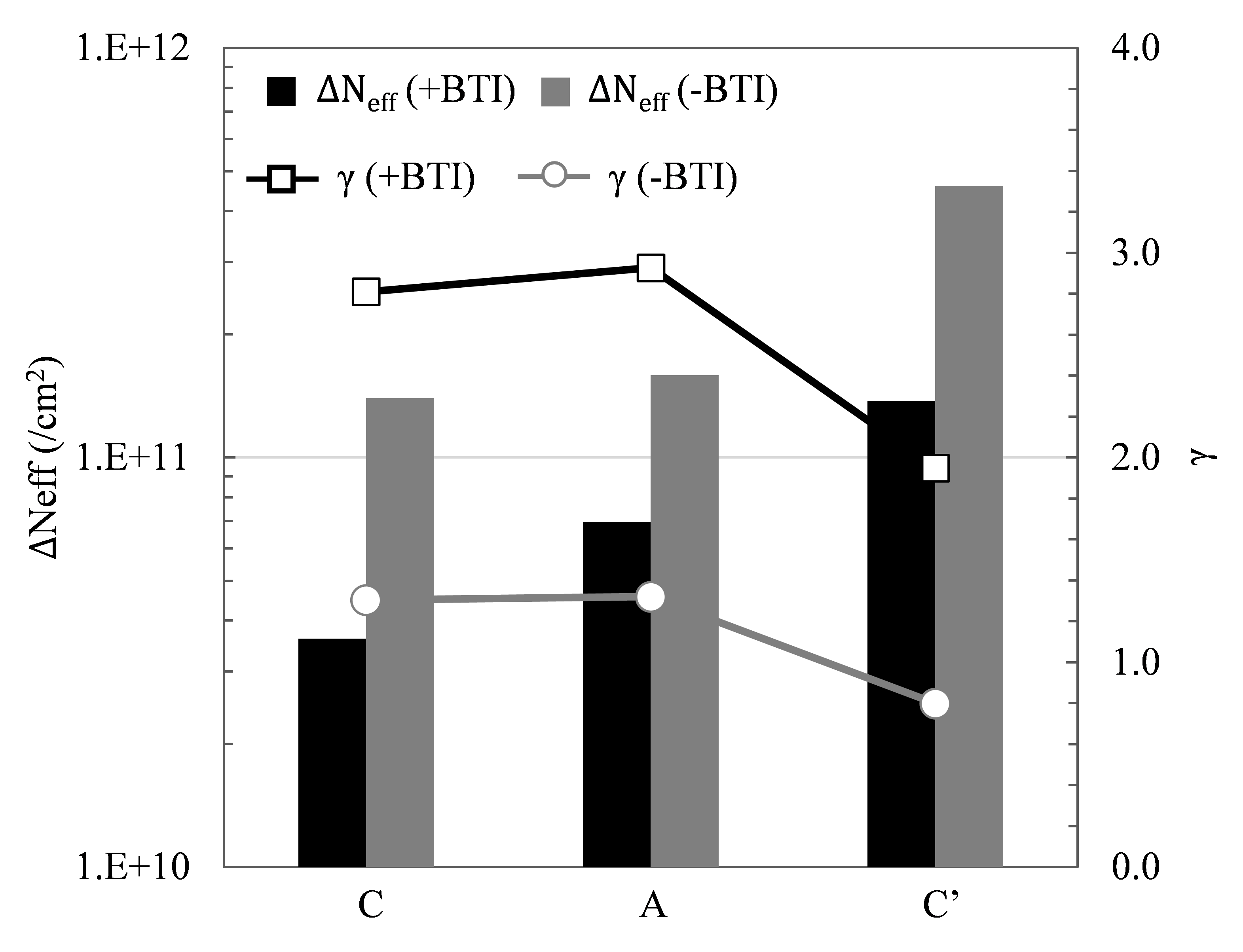 Figure 20 ΔNeff and γ extracted from BTI measurements on MOSFETs applying both positive and negative stress conditions. The data from MOSFETs confirm the trends observed on MOSCAPs.
observation in measurement data and modeling results from the MOSCAP data i.e. the IL layer provides the misalignment between the defect levels in the high-κ and the InGaAs Ef while the LaSiOx reduced the total charging oxide defects. At negative stress conditions, the differences are less pronounced.
The extrapolated max Vov and Vun at 10 years are shown in Fig. 21. Benchmarking the max Vov of the newly proposed gate stack against Si gate stacks (Fig. 22) shows that by using the optimized gate stack III-V devices can meet even the more stringent reliability targets used for a scaled Si technology.
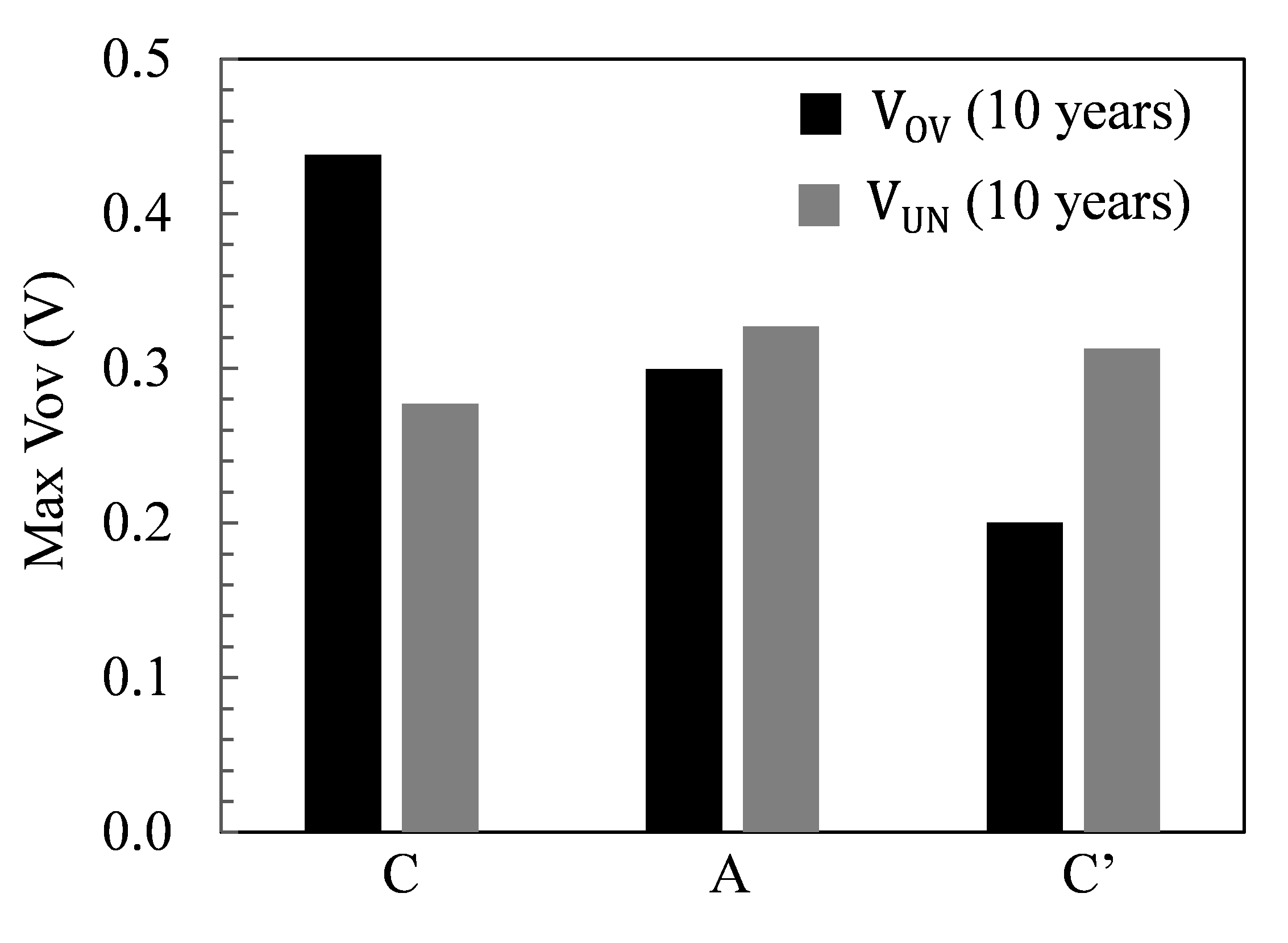 Figure 21. Max Vov and Vun from BTI measurements on MOSFETs with different gate stacks.
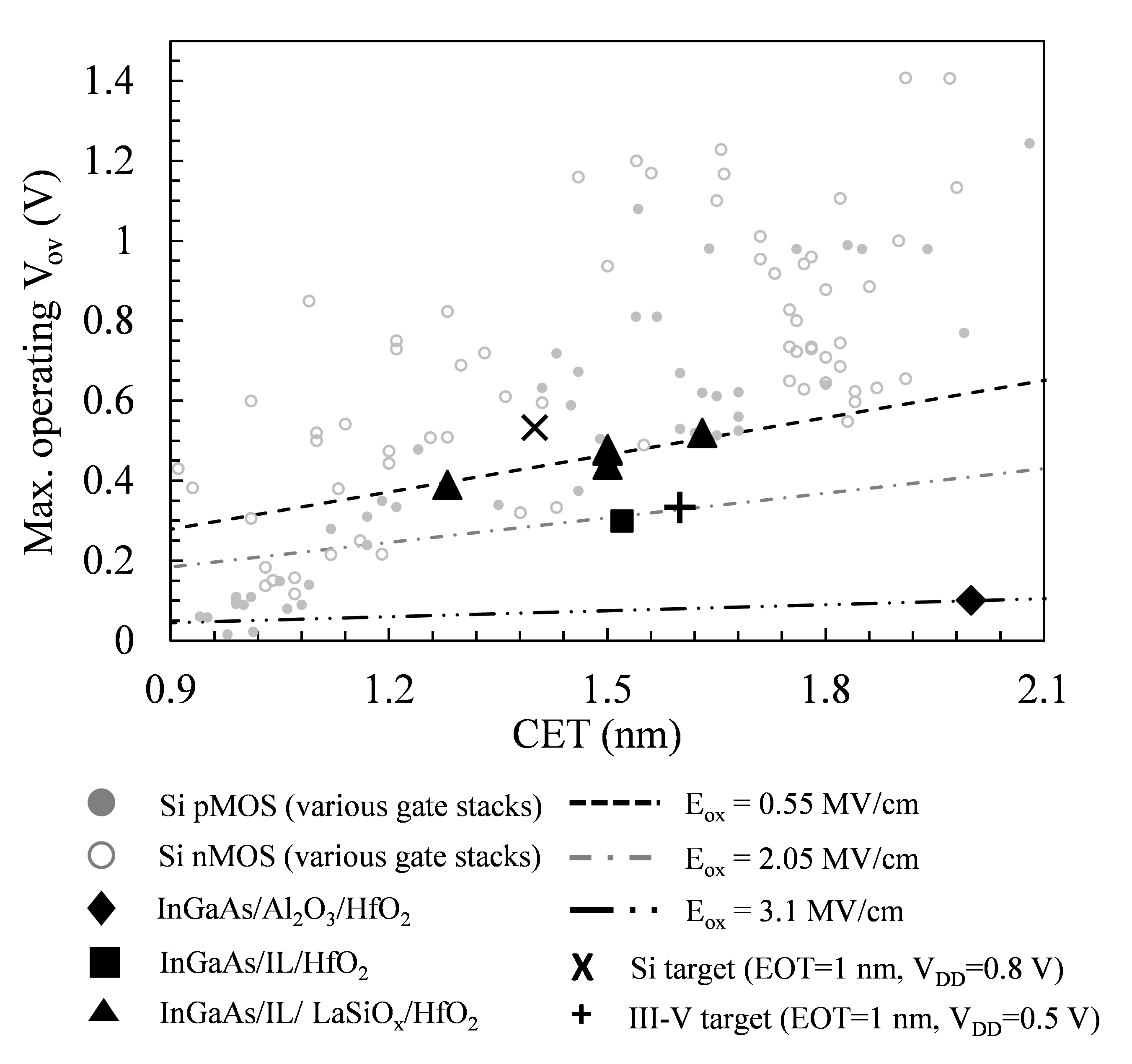 Figure 22. Max. operating overdrive voltage as a function of CET for various gate stacks on Si (p- and n-MOS) and InGaAs. The devices with the IL/LaSiOx/HfO2 gate stack surpass the relability target for III-V semiconductor based technology.
4. Conclusions
We have shown in this work the improved interface and reliability properties of the IL layer. A Dit and ΔNeff reduction are accompanied with a negative Vfb shift and an increase in the value of γ. This suggests the formation of an interface dipole. When a favorable defect band distribution is present as is the case for HfO2, dipole engineering can be applied to misalign the defect band with the InGaAs channel Ef. However, the thermal stability of this stack is limited and a severe intermixing of the IL layer with the InGaAs substrate at typical thermal budget of a IIIV gate stack, degrades the initial improvement seen from the IL layer.
A cap is needed to stabilize this interaction and both Al2O3 and LaSiOx can act as a stabilization layer by La or Al mixing with the IL-layer atoms. While the physical properties are very similar, the electrical properties in terms of oxide traps are very different. The different behavior can be explained by the presence of a broad defect band in Al2O3 making this cap layer not suitable for dipole engineering. On the other hand, LaSiOx shows a more favorable defect band distribution and a further reduction of the oxide defects is observed. In addition, the interface properties are improved and low CET (~1.5 nm) was maintained.
Excellent device characteristics were demonstrated combining the IL passivation layer with the bi-layer stack consisting of 1 nm LaSiOx/3 nm HfO2. III-V devices with record mobility and record reliability performance at scaled EOT were demonstrated. In addition, we show that this stack can be further scaled down to 1nm EOT without loss of performance or reliability.
Conflict of Interest
The authors declare no conflict of interest.
- S. Sioncke, J. Franco, A. Vais, V. Putcha, L. Nyns, A. Sibaja-Hernandez, R. Rooyackers, S. Calderon Ardila, V. Spampinato, A. Franquet, J.W. Maes, Q.Xie, M.Givens, F. Tang, X. Jiang, M. Heyns, D. Linten, J. Mitard, A. Thean, D. Mocuta and N. Collaert, “First demonstration of ~3500 cm2/V-s electron mobility and sufficient BTI reliability (max Vov up to 0.6 V) In0.53Ga0.47As nFET using an IL/LaSiOx/HfO2 gate stack”, in IEEE Symposium on VLSI Technology 2017, pp. T38-T39, 2017. https://doi.org/10.23919/VLSIT.2017.7998192
- A. Vais, A. Alian, L. Nyns, J. Franco, S. Sioncke, V. Putcha H. Yu, Y. Mols, R. Rooyackers, D. Lin, J.W. Maes, Q. Xie, M. Givens, F. Tang, X. Jiang, A. Mocuta, N. Collaert, K. De Meyer, A. Thean, “Record mobility (µeff~ 3100 cm2/Vs) and reliability performance (Vov~ 0.5 V for 10yr operation) of In0.53Ga0. 47As MOS devices using improved surface preparation and a novel interfacial layer” in IEEE Symposium on VLSI Technology, pp. 140-141. 2016. https://doi.org/10.1109/VLSIT.2016.7573410
- C. B. Zota, F. Lindelöw, L.-E. Wernersson, and E. Lind. “InGaAs nanowire MOSFETs with ION= 555 µA/µm at IOFF= 100 nA/µm and VDD= 0.5 V” in IEEE Symposium on VLSI Technology, pp. 1-2. IEEE, 2016. https://doi.org/10.1109/VLSIT.2016.7573418
- N. Waldron, S. Sioncke, J. Franco, L. Nyns, A. Vais, X. Zhou, H. C. Lin, G. Boccardi, J. W. Maes, Q. Xie and M. Givens, F. Tang , X. Jiang , E. Chiu, A. Opdebeeck, C. Merckling, F. Sebaai, D. van Dorp, L. Teugels, A. Sibaja Hernandez, K. De Meyer, K. Barla, N. Collaert, A. Thean, “Gate-all-around InGaAs nanowire FETS with peak transconductance of 2200 μS/μm at 50 nm Lg using a replacement Fin RMG flow” in IEEE International Electron Devices Meeting (IEDM), pp. 31-1. IEEE, 2015. https://doi.org/10.1109/IEDM.2015.7409805
- R. Suzuki, N. Taoka, M. Yokoyama, S. Lee, S. H. Kim, T. Hoshii, T. Yasuda, W. Jevasuwan, T. Maeda, O. Ichikawa, N. Fukuhara, M. Hata, M. Takenaka, and S. Takagi, “ 1-nm-capacitance-equivalent-thickness HfO2/Al2O3/InGaAs metal-oxide-semiconductor structure with low interface trap density and low gate leakage current density,” Appl. Phys. Lett. 100(13), 132906-1–132906-3 (2012). https://doi.org/10.1063/1.3698095.
- F Palumbo, M Eizenberg, “Degradation characteristics of metal/Al2O3/n-InGaAs capacitors”, Journal of Applied Physics, 115 (1), 014106 (2014). DOI: https://doi.org/10.1063/1.4861033
- G. Jiao, C. Yao, Y. Xuan, D. Huang, P.D. Ye, and M.-F. Li, “Experimental Investigation of Border Trap Generation in InGaAs nMOSFETs With Al2O3 Gate Dielectric Under PBTI Stress”, IEEE Trans. Electron Dev., 59, pp. 1661-67 (2012). https://doi.org/10.1109/TED.2012.2190417
- I Krylov, B Pokroy, M Eizenberg, and D Ritter, “A comparison between HfO2/Al2O3 nano-laminates and ternary HfxAlyO compound as the dielectric material in InGaAs based metal-oxide-semiconductor (MOS) capacitors”, Journal of Applied Physics, 120 (12), 124505 (2016). https://doi.org/10.1063/1.4962855
- K. Tang, R. Droopad, and P. C. McIntyre. “Border Trap Density in Al2O3/InGaAs MOS: Dependence on Hydrogen Passivation and Bias Temperature Stress”, ECS Trans., 69 (5), pp. 53-60 (2015). https://doi.org/ 10.1149/06905.0053ecst
- C. L. Hinkle, M. Milojevic, B. Brennan, A. M. Sonnet, F. S. Aguirre-Tostado, G. J. Hughes, E. M. Vogel, R. M. Wallace, “Detection of Ga suboxides and their impact on III-V passivation and Fermi-level pinning”, Appl. Phys. Lett. 94, 162101 (2009). https://doi.org/10.1063/1.3120546
- D. Lin, A. Alian, S. Gupta, B. Yang, E. Bury, S. Sioncke, R. Degraeve, M. L. Toledano, R. Krom, P. Favia, H. Bender, M. Caymax, K. C. Saraswat, N. Collaert, A. Thean, ”Beyond interface: The impact of oxide border traps on InGaAs and Ge n-MOSFETs”, in Proceedings of IEEE International Electron Device Meeting Technical Digest, 28.3.1 (2012). https://doi.org/10.1109/IEDM.2012.6479121
- S. Deora, G. Bersuker, W.-Y. Loh, D. Veksler, K. Matthews, T. W. Kim, R. T. P. Lee, R. J. W. Hill, D.-H. Kim, W.-E. Wang, C. Hobbs, P. D. Kirsch, “Positive Bias Instability and Recovery in InGaAs Channel nMOSFETs”, IEEE Transactions on Device and Materials Reliability, 13(4), 507 (2013). https://doi.org/10.1109/TDMR.2013.2284376
- J. Franco A. Alian, B. Kaczer, D. Lin, T. Ivanov, A. Pourghaderi, K. Martens, Y. Mols, D. Zhou, N. Waldron, S. Sioncke, T. Kauerauf, N. Collaert, A. Thean, M. Heyns, and G. Groeseneken, “Suitability of high-k gate oxides for III-V devices: a PBTI study in In0.53Ga0.47As devices with Al2O3”, in Proceedings of IEEE International Reliability Physics Symposium Technical Digest, 6A.2.1 (2014). https://doi.org/ 10.1109/IRPS.2014.6861098
- N. Conrad, M. Si, S. H. Shin, J. J. Gu, J. Zhang, M. A. Alam, P. D. Ye, “Low-frequency noise and RTN on near-ballistic III–V GAA nanowire MOSFETs”, in Proceedings of IEEE International Electron Devices Meeting, 20.1.1 (2014). https://doi.org/10.1109/IEDM.2014.7047086
- N. Taoka, M. Yokoyama, S. H. Kim, R. Suzuki, S. Lee, R. Iida, T. Hoshii, W. Jevasuwan, T. Maeda, T. Yasuda, O. Ichikawa, N. Fukuhara, M. Hata, M.Takenaka and S. Takagi, “Impact of Fermi Level Pinning Due to Interface Traps Inside the Conduction Band on the Inversion-Layer Mobility in InGaAs Metal–Oxide–Semiconductor Field Effect Transistors”. IEEE Trans. Dev. Mat. Rel. 13, 456 (2013). https://doi.org/10.1109/TDMR.2013.2289330.
- S. Stemmer, V. Chobpattana, and S. Rajan, “Frequency dispersion in III-V metal-oxide-semiconductor capacitors”, Appl. Phys. Lett. 100, 233510 (2012). https://doi.org/10.1063/1.4724330.
- S. . Johansson, M. Berg, K. M. Persson and E. Lind, “Transconductance method for characterization of border traps”, IEEE Trans. Electron Devices, vol. 60, no. 2, February 2013. https://doi.org/ 10.1109/TED.2012.2231867
- J. Franco, B. Kaczer, Ph. J. Roussel, J. Mitard, S. Sioncke, L. Witters, H. Mertens, T. Grasser, and G. Groeseneken, “Understanding the suppressed charge trapping in relaxed-and strained-Ge/SiO2/HfO2 p-MOSFETs and implications for the screening of alternative high-mobility substrate/dielectric CMOS gate stacks” in Proceedings of IEEE International Electron Devices Meeting, 15.2.1 (2013). https://doi.org/ 10.1109/IEDM.2013.6724634
- J. Franco, A. Vais, S. Sioncke, V. Putcha, B. Kaczer, B-S. Shie, X. Shi, R. Mahlouji, L. Nyns, D. Zhou, and N. Waldron, “Demonstration of an InGaAs gate stack with sufficient PBTI reliability by thermal budget optimization, nitridation, high-k material choice, and interface dipole” in 2016 IEEE Symposium on VLSI Technology, , pp. 1-2., 2016. https://doi.org/ 10.1109/VLSIT.2016.7573371
- A. Alian, M. A. Pourghaderi, Y. Mols, M. Cantoro, T. Ivanov, N. Collaert, and A. Thean, “Impact of the channel thickness on the performance of ultrathin InGaAs channel MOSFET devices”, in Proceedings of IEEE International Electron Device Meeting, pp.16.6.1-16.6.4, 2013. https://doi.org/ 10.1109/IEDM.2013.6724644
- E. H. Nicolian and J. R. Brews, MOS Phys. and Tech., p. 215-216, Wiley Interscience, New York (2003).
- R. Winter, J. Ahn, P. C. McIntyre, and M. Eizenberg, “New method for determining flat-band voltage in high mobility semiconductors”, Journal of Vacuum Science & Technology B 31, 030604 (2013). https://doi.org/ 10.1116/1.4802478
- D. K. Schroder, Semiconductor material and device characterization. John Wiley and Sons, 2006, ISBN: 978-0-471-73906-7.
- B. Kaczer, T. Grasser, P.J. Roussel, J. Martin-Martinez, R. O’Connor, B. O’Sullivan, and G. Groeseneken, “Ubiquitous relaxation in BTI stressing—New evaluation and insights” in proceedings of IEEE International Reliability Physics Symposium, 2008, pp. 20-27, 2008. https://doi.org/ 10.1109/RELPHY.2008.4558858
- A. Vais, J. Franco, H.-C. Lin, N. Collaert, A. Mocuta, K. De Meyer, and A. Thean, “Impact of starting measurement voltage relative to flat-band voltage position on the capacitance-voltage hysteresis and on the defect characterization of InGaAs/high-k metal-oxide-semiconductor stacks”, Appl. Phys. Lett. 107, 223504 (2015). https://doi.org/ 10.1063/1.4936991
- V. Putcha, J. Franco, A. Vais, B. Kaczer, S. Sioncke, D. Linten and G. Groeseneken, “Impact of slow and fast oxide traps on In0.53-Ga0.47As device operation studied using CET maps”, in proceedings of IEEE International Reliability Physics Symposium 2017, XT-8.1 (2017). https://doi.org/ 10.1109/IRPS.2018.8353603