Improvement of Transmission Characteristics in Multilayer Dual Band Filter

Adv. Sci. Technol. Eng. Syst. J. 3(5), 16–22 (2018);
 DOI: 10.25046/aj030503
This paper first simplifies the GA-optimized filter structure developed by us. Then the filter structure is modified by introducing slot and conductor stubs, based on electric fields and magnetic currents at resonant and transmission zero points. As a result, return losses in two passband regions are suppressed more than 28 dB, and also insertion loss in stopband dividing two passbands is suppressed more than 20 dB. Finally, two kinds of the proposed filters are fabricated, and effectiveness of them is confirmed from comparison between the measured and the numerical results.
1. Introduction
This paper is an extension of work originally presented in 2017 Asia Pacific Microwave Conference, (APMC2017) [1]. Based on our work in [2], the goal is to develop high-performance UWB bandpass filter.
In recent years, wireless communication systems such as wireless local area network (LAN) and mobile terminals have spread rapidly. High-frequency filters are used to extract a signal of a desired frequency band for the purpose of prevention of unnecessary radiation and interference. Increasing in complexity and volume of wireless communication, a filter having a large attenuation amount close to pass band and an improved insertion loss is indispensable. Conventional resonant elements that have been developed to achieve high performance such as improved multi-band sharing and attenuation characteristics outside a pass band required for the wireless communication device are not sufficient. Therefore, development of a new resonant element desired. Under such circumstances, we have proposed the ultra-wideband (UWB) filter, of which conductor patches and slot shapes were optimized under the genetic algorithm (GA) technique [2]. As for UWB filters, many filter structures have been developed [3-17]. They are essentially based on the multi-mode resonators (MMR) which were first developed in [3]. Then, various stub-loaded resonators were often used to achieve good skirt selectivity and compact size [4-7]. To perform further good filter performance, the resonator shapes including a stepped-impedance technique were investigated [8-17]. The planar circuit filter designed by GA shows the desired characteristics according to the evaluation function, but the return loss there was not so high (about 10 dB). In addition to the problem of calculation capacity and computation time, the circuit element shape is complicated and the degree of freedom is small, so that it is difficult to improve the filter characteristics by slightly modifying the GA-optimized filter shape.
In this work, we clarify resonant mechanism and transmission zero mechanism of the UWB filter optimized by the GA. Then, the simplified filter structure based on the their mechanisms is proposed. Furthermore, to improve loss characteristics between two passbands of the dual-band filter, the conductor and slot stubs are newly loaded. Validity of the proposed filter is also verified experimentally.
The rest of this paper is structured/organized as follows: Section 2 discusses resonant mechanism of the UWB filter; Section 3 presents improvement of filter transmission characteristics; Section 4 verifies effectiveness of the proposed filter; and finally, in Section 5, we summarize the conclusions derived from this work and indicate possible future works.
2. Simplified filter generated by GA
New planar circuit filters have been developed by GA evaluated characteristics of both passband and stopband [18-19]. In this section, we briefly describe the structure of the multilayer planar circuit filter and the outline of the optimized design by the GA of the planar circuit filter [18-19]. After the circuit shape and filter characteristics are described, we simplify the filter based on resonant principle.
2.1. Structure of the GA-optimized UWB filter
Figure 1 shows the UWB-filter structure developed by us. This filter optimized by GA consists of slot elements on the ground plane and patch elements on the conductor-backed dielectric substrate (er = 2.2, thickness t2 = 0.51 [mm]). Both elements have arbitrary shapes and the filter is covered by the shielding box (a = b = 15.2 [mm], c = 20.0 [mm]). Input and output of the filter are connected through a microstrip line. A lot of resonances are mainly caused by slot elements.
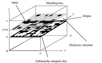 Figure 1. Structure of the GA-optimized UWB filter.
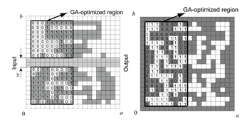 Figure 2. An example of an arbitrarily-shaped element constructed by uniform mesh.
2.2. Shape of the GA-optimized UWB filter
As shown in Fig. 2, the planar circuit shape is represented by a set of conductor patch cells and handled by binary codes of “0” and “1” in the optimized design method by GA [3]. The analysis is performed by the moment method. In the design, the symmetrical structure on the plane of is assumed and the shape of the input/output line is fixed. The parameters for optimization by GA are set as follows. The planes at z = t1 and t1 + t2 are divided into 20×20 cells, and the size of one cell is 0.76 mm. The evaluation frequency bands are 3.4-4.8 GHz, and 7.25-10.25 GHz in the passband, while 1.0-3.0 GHz, 5.0-7.0 GHz, and 10.35-14.0 GHz in the stopband, and the target of the return loss in the passband and the insertion loss in the stopband are set as 10dB. The mutation rate is 0.02 and the crossover rate is 0.8. The generation number is 400, the population size of one generation is 50, and the elitist strategy is applied.
Figure 3 (a) and (b) show the optimized patch and slot shapes, respectively and Fig. 4 shows its transmission characteristics. It is found that the passbands in the low and high frequency ranges are constituted by five resonances. Since the circuit shape obtained from GA is very complicated, it is very difficult to modify its shape for improving the filter characteristic. Therefore, the resonant principle is clarified from the electric-field distribution, and the shape is simplified based on this.
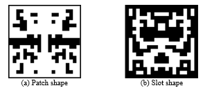 Figure 3. Shape of the GA-optimized UWB filter.
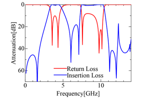 Figure 4. Frequency characteristics of the UWB filter optimized by GA.
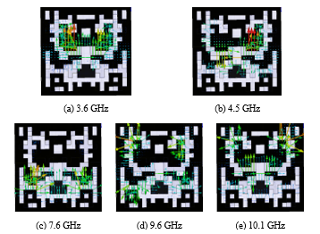 Figure 5. Electric-field distribution at each resonance.
2.3. Resonant mechanism
Resonances are mainly caused on the slot face, so we observe the electric-field distributions on the slots. Figure 5 shows the electric field on the slot at each resonant point. Resonance at 3.6 GHz shown in Fig. 5 (a), is the half-wavelength even resonant mode of the upper-part slot. Resonance at 4.5 GHz in Fig. 5 (b) is the half-wavelength odd resonant mode of the two slots arranged symmetrically for the center line. Resonance at 7.6 GH in Fig. 5 (c) is the half-wavelength even resonant mode of the lower-part slot. Resonance at 9.6 GHz in Fig. 5 (d) is the odd resonant mode that is the next higher-order one of the resonance at 4.5 GHz. Resonance at 10.1 GHz in Fig. 5 (e) is the 3/2-wavelength even resonant mode that is the higher-order one of the resonance at 3.6 GHz. From the above-mentioned guess of the resonant mechanism, we first calculate the frequency characteristics for the simplified structure shown in Fig. 6 (a) and (b). Its frequency characteristic is shown in Fig. 7, where four
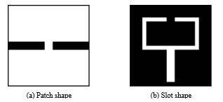 Figure 6. Basic structure of the upper-part slot.
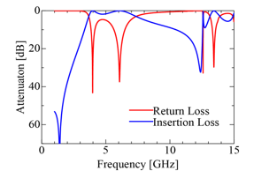 Figure 7. Frequency characteristic of the simplified slot structure shown in Fig.6.
 Figure 8. Basic structure of the lower-part slot.
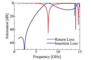 Figure 9. Frequency characteristic of the simplified slot structure shown in Fig.8.
resonant points are produced corresponding to the first, the second , the forth and the fifth resonant points in Fig. 4. Figures 8 (a) and (b) also show another simplified structure and its frequency characteristic is given in Fig. 9, where one resonant point is produced corresponding to the third resonance in Fig. 4. Then we combine these two basic simplified structures and adjust the filter characteristics to the UWB filter by adding slot stubs and microstrip patches and also by modifying the slot junction part. As a result, Fig. 10 (a) and (b) are obtained as a simplified filter structure and the enlarged part of the slot junction is also shown in Fig.10 (c) The dimensions are listed in Table 1. The slot width is 0.76 mm. Figure 11 shows the frequency characteristics of the simplified UWB filter. Five resonances are reproduced near the original resonant frequencies shown in Fig. 4. Figure 12 shows the magnetic currents at the resonant point to confirm the resonant mechanism. It is clear from this figure that the simplified filter structure works by the same resonant mechanism with that of the GA optimized filter. However, the insertion loss in the stopband is not so high less than 20 dB. So we improve it by considering mechanism of the transmission zeros in the next session.
Table 1. Dimensions of the patch and the slot parameters (unit: mm).
| = 1.52 | = 0.76 | = 1.78 | = 2.24 | = 3.61 |
| = 1.04 | = 1.52 | = 2.78 | = 2.38 | = 4.90 |
| = 1.42 | = 0.74 | = 2.58 | g = 0.74 | = 2.58 |
| = 3.04 | = 6.84 | = 10.64 | = 3.80 | = 4.56 |
| = 13.68 | = 5.80 | = 1.06 | = 1.47 | = 1.4 |
| = 3.06 | = 0.46 | The slot width is 0.76 mm | ||
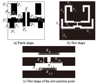 Figure 10. Shape of the simplified UWB filter.
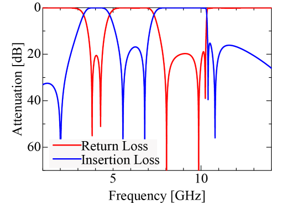 Figure 11. Frequency characteristics of the simplified filter.
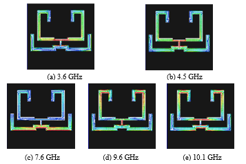 Figure 12. Magnetic-current distribution at each resonance.
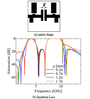 Figure 13. Frequency for various gap g.
 Figure 14. Magnetic-current distribution at 5.5 GHz.
3. Improvement of stopband characteristics
We can see five transmission zeros within 12 GHz in Fig. 4. Among these transmission zeros, the first and second zeros can control by slight modifications of the filter shape, which have little influence for the passband characteristics. We first take notice of the transmission zero at 2.0 GHz. This transmission zero may be caused by the cancellation due to the direct coupling between the input and the output microstrip line through the gap g shown in Fig. 13 (a). Figure 13 (b) shows the transmission characteristics for varying the value of the gap g. As expected, only the first transmission zero greatly moves, depending on g. It is clear that the gap g is a useful parameter for controlling the frequency point
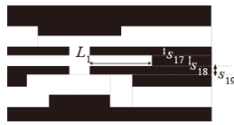 Figure 15. Parameters of the slot stub.
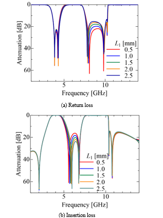 Figure 16. Frequency characteristics for various slot stub length L1.
of the first transmission zero. Next, we notice of the second transmission zero of 5.5 GHz. Figure 14 shows the magnetic-current distribution at 5.5 GHz. We can see from this figure that the magnetic current strongly flows in the center slot connecting between the lower-part and higher-part slots. Therefore, if the slot stub is loaded into the center slot, the transmission zero at 5.5 GHz can move independently.
Figure 15 shows the slot stub of the length L1 and the other parameters are s17 = 0.33 [mm], s18 = 0.30 [mm], s19 = 0.33 [mm]. Figure 16 shows the frequency characteristics for varying L1. Although only the second zero point shifts to the higher frequency region with increasing L1 and the stopband characteristic is improved as expected, the third resonant point also moves to the higher region, and the passband characteristic slightly deteriorates. The third resonance at 7.6 GHz is generated by the bottom slot as mentioned in Sec. 2, but if the length of the resonator is made longer, the second and the forth resonances also a little bit move, so such a deformation of the bottom slot for characteristic improvement is difficult. Therefore, we install a small projection of the length in the upper slot resonator shown in Fig. 17. The projection is coupled with the lower slot resonator so that only the
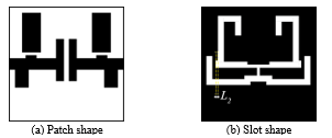 Figure 17. Shape of the filter with an additional projection of the length.
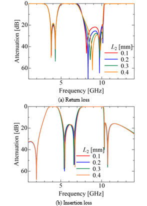 Figure 18. Filter characteristics for various projection length L2.
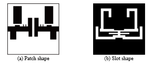 Figure 19. Proposed filter structure loading two conductor stubs.
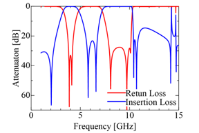 Figure 20. Filter characteristics of the proposed filter.
third resonance can move. Figure 18 shows the transmission characteristics for varying value of L2. Clearly only the third resonance moves and other resonances, and the transmission zero points don’t move. Furthermore, two small conductor stubs are loaded on the input/output line in order to improve the transmission characteristics at around 10 GHz as shown in Fig. 19. Figure 20 shows the transmission characteristics of the filter proposed under the above-mentioned investigation and, the return losses in the two passbands are suppressed to 28 dB, and the insertion loss in the stopband is suppressed to 20 dB or more. Most of UWB filters do not reach to these-losses levels in three pass and stop bands.
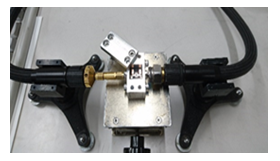 Figure 21. Measurement system.
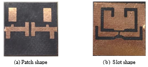 Figure 22. Photograph of the simplified filter.
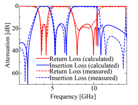 Figure 23. Measurement frequency characteristics of the simplified filter.
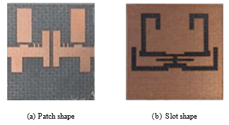 Figure 24. Photograph of the proposed filter.
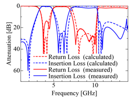 Figure 25. Measured frequency characteristics of the proposed filter.
4. Experimental results
To confirm effectiveness of the proposed filters, we fabricate two kinds of them by the photo-etching technique. As a dielectric substrate, we use Rogers RT/duroid 5880 with dielectric constant er = 2.2 and the thickness t2 = 0.508 [mm], and also measure the filter characteristics in the shielding box (see the photograph of the measurement system in Fig. 21) by the vector network analyzer (Agilent Technologies Inc. E8361C). The first fabricated filter has the simplified structure shown in Fig. 10 and its photograph is shown in Fig. 22. Comparison of the transmission characteristics between the measured and the calculated results are performed in Fig. 23, where the solid lines indicate the measured results and the dashed lines are the calculated ones. Both results are in good agreement with each other in the insertion and the return losses. The return losses in the two passbands are suppressed to 15 dB, and the insertion loss in stopband is also suppressed to 15 dB. On the other hand, the second fabricated filter has the structure with further improvement of the filter characteristic shown in Fig. 20 and its photograph is shown in Fig. 24. The measured results of the transmission characteristics indicated by the solid lines are compared with the calculated ones of the dashed lines in Fig. 25. The measured return loss in the low-frequency passband is about 15 dB lower that the calculated one, whereas that in the high-frequency passband is more than 20 dB and also the measured insertion loss in the stopband dividing two passbands is more than 25 dB. Although there is some deviation between both results due to the fabrication error for the small patch stubs and the slot stub added to the simplified structure. We can confirm the obvious improvement of the filter characteristics experimentally.
5. Conclusion
In this paper, we have clarified from the electric fields that two passbands in the GA-optimized filter developed by us are constructed by five resonant modes and have proposed the simplified structure based on the resonant mechanism. For further improvement of the simplified filter, the mechanism of the transmission zero is investigated from distributions of the magnetic currents. So that by newly loading both the slot stub and the conductor stub, the return loss more than 28 dB in two passbands and also the insertion loss more than 20 dB in the stopband in between passbands have been achieved. Finally, effectiveness of the proposed filter has been verified experimentally. To suppress spurious responses in the frequency region more than 14 GHz is the future work, although we don’t investigate it in this paper.
Conflict of Interest
The authors declare no conflict of interest.
Acknowledgment
This work was supported in part by a Grant-in-aid for Scientific Research(C) (16K06372) from Japan Society for the Promotion of Science.
- Y. Takeuchi, R. Nakano, H. Deguchi, M. Tsuji “Improvement of transmission characteristics in multilayer dual band filter,” 2017 IEEE Asia Pacific Microwave Conference (APMC) 13-16, Nov. 2017 https://doi.org/10.1109/APMC.2017.8251528.
- T. Kido, H.Deguchi, M.Tsuji “Compact planar bandpass filters with arbitrarily-shaped conductor ptches and slots,” IEICE Trans. Electron., vol. E94-C, no. 6 pp.1091-1097, June 2011 https://doi.org/10.1587/ transele.E94.C.1091.
- L. Zhu, S. Sun, W. Menzel “Ultra-wideband (UWB) bandpass filters using multiple-mode esonator,” IEEE Microw. Wireless Compon. Lett., vol. 15, no. 11, pp. 796-798, Nov. 2005 https://doi.org/10.1109/LMWC.2005.859011.
- R. Li, L. Zhu, “Compact UWB bandpass filter using stub-loaded multiple-mode resonator,” IEEE Microw. Wireless Compon. Lett., vol. 17, no. 1, pp. 40-42, Jan. 2007 https://doi.org/10.1109/LMWC.2006.887251.
- L. Han, K. Wu, X.P. Chen, “Compact ultra-wideband bandpass filter using stub-loaded resonator,” Electron. Lett., vol. 45, no. 10, pp. 504-506, May 2009 https://doi.org/10.1049/el.2009.0510.
- Y. Zhou, B. Yao, Q. Cao, H. Deng, X. He, “Compact UWB bandpass filter using ring open stub loaded multiple-mode resonator,” Electron. Lett., vol. 45, no. 11, pp. 554-556, May 2009 https://doi.org/ 10.1049/el.2009.3724.
- H. W. Deng Y. J. Zhao L. Zhang X. S. Zhang S. P. Gao “Compact quintuple-mode stub-loaded resonator and UWB filter,” Progress In Electromagnetics Research Letters., vol14, no. 8, pp. 111-117, 2010 https://doi.org/10.2528/PIERL10030912.
- K. Song, Q. Xue, “Novel broadband bandpass filters using Y-shaped dual-mode microstrip resonators,” IEEE Microw. Wireless Compon. Lett., vol. 19, no. 9, pp. 548-590, Sept. 2009 https://doi.org/10.1109/LMWC.2009.2027058.
- L. Han, K. Wu, X. Zhang, “Development of packaged ultra-wideband bandpass filters” IEEE Trans. Microw. Theory Tech., vol. 58, no. 1, pp. 220-228, Jan. 2010 https://doi.org/10.1109/TMTT.2009.2036399.
- Q.-X. Chu, X.-K. Tian, “Design of UWB bandpass filter using stepped-impedance stub-loaded resonator,” IEEE Microw. Wireless Compon. Lett., vol. 20, no. 9, pp. 501-503, Sept. 2010 https://doi.org/10.1109/LMWC.2010.2053024.
- J. Xu, W. Wu, W. Kang, C. Miao, “Compact UWB bandpass filter with a notched band using radial stub loaded resonator,” IEEE Microw. Wirel. Compon. Lett,. vol. 22, no. 7, pp. 351-353, July 2012 https://doi.org/10.1109/LMWC.2012.2201930.
- Z.X. Zhang, F. Xiao, “An UWB bandpass filter based on a novel type of multi-mode resonator,” IEEE Microw. Wirel. Compon. Lett., vol. 22, no. 10, pp. 506-508, Oct. 2012 https://doi.org/10.1109/LMWC.2012.2218229.
- H. Zhu, Q.-X. Chu, “Compact ultra-wideband (UWB) bandpass filter using dual-stub-loaded resonator (DSLR),” IEEE Microw. Wireless Compon. Lett., vol. 23, no. 10, pp. 527-529, Oct. 2013 https://doi.org/10.1109/LMWC.2013.2278278.
- L.C. Lin, S. Yang, S.J. Sun, C.H. Liang, “Ultra-wideband bandpass filter using multi-stub-loaded ring resonator,” Electron. Lett., vol. 50, no. 17, pp. 1218-1220, Aug. 2014 https://doi.org/10.1049/el.2014.1256.
- X. Li, X. Ji, “Novel compact UWB bandpass filters design with cross-coupling between short circuited stubs,” IEEE Microw. Wirel. Compon. Lett., vol. 24, no. 1, pp. 23-25, Jan. 2014 https://doi.org/10.1109/LMWC.2013.2287231.
- A. Taibi, M. Trabelsi, A. Slimane, M. T. Belaroussi, J. P. Raskin, “A novel design method for compact UWB bandpass filters,” IEEE Microw. Wireless Compon. Lett., vol. 25, no. 1, pp. 4-6, Jan. 2015 https://doi.org/10.1109/LMWC.2014.2363016.
- S. Kumar, R. D. Gupta, M. S. Parihar, “Multiple band notched filter using C-shaped and E-shaped resonator for UWB applications,” IEEE Microw. Wireless Compon. Lett., vol. 26, no. 5, pp. 340-342, May 2016 https://doi.org/10.1109/LMWC.2016.2549700.
- M. Tsuji, H. Deguchi, A. Kido, M. Ohira “Multi-resonator generation by genetic optimization for application to panar-circuit bandpass filters,” Special issue on recent progress in computational electro magnetics and its applications. Volume 129 (2009) Issue 10 Pages 681-686 https://doi.org/10.1541/ieejfms.129.681
- A. Kido, H. Deguchi, M. Tsuji, M. Ohira “Multi-resonator generation in arbitrarily-shaped planar-circuit filters by genetic optimization,” 2007 European Microwave Integrated Circuit Conference 8-10 Oct. 2007 https://doi.org/10.1109/EMICC.2007.4412744