Synthesis of QDI Combinational Circuits using Null Convention Logic Based on Basic Gates
 , Orlando Verducci 1, Vitor Leandro Vieira Torres 1, Robson Moreno 2, Lester de Abreu Faria 1
Adv. Sci. Technol. Eng. Syst. J. 3(4), 308–317 (2018);
 DOI: 10.25046/aj030431
Currently, synchronous digital circuits (SDC) may require certain design conditions, such as power consumption, robustness, performance, etc. These design conditions are more difficult to satisfy when SDC are implemented in VLSI (Very Large Scale Integration) technology and in the deep-sub-micron MOS (DSM-MOS) technology. The asynchronous design style has properties that serve as an alternative to design DSM-MOS technology circuits and it can satisfy these design conditions. Quasi Delay-Insensitive (QDI) circuits is a class of asynchronous circuits, they have properties where the DSM-MOS technology design is applied, because they are robust to noise, temperature and voltage variations, as well as low electromagnetic emissions, and they are tolerant to certain faults. An interesting style of QDI combinational circuits are NCL (NULL Convention Logic) circuits, because they accept conventional Boolean functions and it can achieve a better optimization. This paper presents an approach and an architecture based in basic gates for the synthesis of NCL gates, therefore its implementation uses only standard libraries and Field Programmable Gate Array (FPGA). The proposed QDI combinational circuits are implemented in the approach that uses only NCL gates.
1. Introduction
This paper is an extension of work originally presented in 2017 IEEE XXIV International Conference on Electronics, Electrical Engineering and Computing (INTERCON) [1].
Synchronous digital circuits are quite popular and conventionally use a global clock to synchronize their operations. The reason for this popularity is the simplicity of the design. There is also an abundant offer of commercial EDA (Electronic Design Automation) tools for their automatic synthesis. Synchronous circuits have been implemented in deep-sub-micron MOS (DSM-MOS) technology, but global clock signal leads to different problems of synchronous design, such as: a) less tolerance to noise and electromagnetic interaction which increase due to high clock frequency; b) distributing of clock signal is increasingly difficult; c) rise in the delay time variation (Tp-MAX, Tp-MIN) in a gate or wire results in loss of performance, because clock must be adjusted to the maximum delay; d) intensification of drivers amount in the clock signal, consuming a significant part of total energy; e) aggravation of the clock skew; and f) significant delay in wires causes an increase in time analysis complexity [2].
The asynchronous paradigm is a promising alternative to digital design because it eliminates problems related to clock signal and also it increases the robustness of circuits. These circuits operate by events, so there is no overall signal to synchronize operations. Synchronization in asynchronous circuits is performed by protocols of type handshake. In the asynchronous paradigm, there are different classes of asynchronous circuits [3]. The class is defined by its delay model in which the circuit operates correctly and by its operation mode in which it describes how communication works with the environment [4]. The delay models can be classified, such as: a) Bounded Gate and Wire Delay which is similar to the synchronous paradigm [2]; and b) Unbounded Gate and Wire Delay (UGWD). In the UGWD model, the delays of gates and wires can be undefined (any delay value), but finite. In this class, we have the delay-insensitive (DI) circuits that are free of timing analysis. Martin [5,6] shows that DI circuits are very restricted. They can only be synthesized using C elements and inverting gates. Two less restricted variants of the UGWD model are: b1) speed-independent (SI) circuits that obey the model in which it has as restriction the delay in wires equal to zero, i.e., the unbounded gate delay and zero wire delay model [3]; and b2) quasi delay-insensitive (QDI) circuits, they have as a constraint the delays in wires when they form a fork, i.e., wires with fan-out > 1 must have approximately equal delays [4,6], so QDI circuits obey the UGWD model and isochronic fork constraint. The interaction of these circuits, for example, DI, SI, QDI with the environment is performed in the I/O_M mode [3, 4, 6]. In I/O_M mode, any change in the output signal can immediately activate a change in the input signal.
For DSM-MOS technology, the asynchronous circuits that best meet the requirements of digital design are the QDI circuits [7]. The QDI circuits have important properties, such as: a) potential to have better latency time, because it works with real delays and not with maximum delays; b) greater robustness to PVT (variations of Process, supply Voltage and Temperature); c) greater robustness to interaction with environment and Stuck-at faults (class of faults tested easily); d) it allows high reuse, because they are highly modular, so they can be used as intellectual property – IP [8]; e) better performance in design of security systems (e.g., encryption) [9]; and f) highly simplified timing analysis.
In QDI combinational circuits (QDI_CC), the data are represented by DI codes of type m-of-n and the most usual processing is the “4-phase” protocol. Several styles were proposed for the synthesis of QDI_CC [10-31]. Firstly, we quote the Minterm Insensitive Delay Synthesis (DIMS) [12] which is quite popular because of its simplicity, but it has a large overhead in area. In DIMS functions, products are implemented with C- elements. Figure 1a shows the operations table of C-element, Figure 1b and 1c show implementations as semi-static CMOS and basic gates, respectively. Another style is the NULL Convention Logic (NCL) proposed by Kant et al. [13]. The NCL style is based on a set of 27 complex gates implemented at the CMOS transistor level [14, 15]. The method for designing QDI_CC based on NCL gates departs from conventional minimized Boolean functions that are transformed into dual-rail Boolean functions and then, the technological mapping is performed using an NCL gates library [16]. The QDI_CC style based on NCL gates has the difficulty of implementing NCL gates in programmable devices, such as Field Programmable Gate Array (FPGAs) [21, 22], while for Very Large Scale Integration (VLSI) it is used standards libraries.
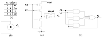 Figure 1. C-element: a) table of operation; b) symbol; c) semi-static version; d) version based on basic gates.
The operating table of NCL gates, not considering the weights, is shown in Figure 2a. The symbol for an THmn NCL gate is shown in Figure 2b, where n is the input number and m represents the minimum number of inputs that are activated with value one, so that the output is activated with value one. For output to be enabled at zero, all n inputs must be enabled at zero. For illustration, the TH23 NCL gate shown in Figure 3 has been implemented in static CMOS technology. In [17-20] three basic gates architectures that implement NCL threshold gates have been proposed for applications that involve standard-cell VLSI or FPGA platforms. In order to operate correctly, these architectures must obey the fundamental mode (FM), therefore they are not QDI.
The interaction with the environment proposes that in the FM mode, “for a new activation of some input signal, the circuit must be stabilized in a stable state, therefore without any electrical activity” [1]. The C-element implemented with basic gates, as shown in Figure 1c, is not QDI because when Q goes from 0 to 1, the circuit must satisfy the fundamental mode to change the inputs again. The QDI_CC design styles of [11, 26-31] are based on basic gates, but they use additional circuits to detect the indicatability which is the requirement to be free of timing analysis.
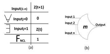 Figure 2. THmn NCL gates: a) table of operations; b) symbol.
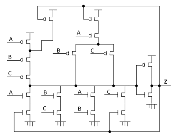 Figure 3. TH23 NCL gate of [16].
To implement THmn NCL gates, this paper proposes a new architecture based on basic gates (see Figure 4). The resulting NCL gates operate in I/O_M mode, therefore they are QDI. Because the NCL gates library is synthesized with only basic gates, then these NCL gates can be easily mapped to platforms of type FPGA or type standard-cell VLSI. This paper also proposes an approach that synthesizes Boolean QDI functions with strong indication using only proposed NCL gates.
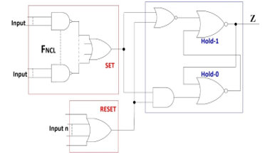 Figure 4. Proposed architecture for THmn NCL gates.
2. Synthesis of NCL Gates: Overview
In order to implement NCL gates, different architectures were proposed at the transistor level [14, 15]. We can also cite architectures that use basic gates, such as proposals [1, 17]. The architecture of [17] is based on Huffman’s machine, and the architecture of [1] uses RS latches, which is a semi-static CMOS version of [15].
2.1. Synthesizing Huffman machines as NCL gates
The implemented THmn NCL gates in the Huffman machine architecture [17-20] (see Figure 5) can be synthesized by the Huffman method [3]. We chose the NCL TH23 gate to illustrate method and architecture. The first step of design procedure started with the generation of operations table from the Z function of TH23 NCL gate, as shown in Figure 6a, its function being Z = AB + AC + BC. In the second step, the operations table is represented in the Karnaugh map. In final step, it is realized conventional logic minimization, extracting next-state equations Z(t+1), shown in Figure 6b. The final Z(t+1) equation was extracted by an algebraic manipulation. The logic circuit of TH23 gate is shown in Figure7.
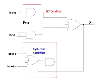 Figure 5. Architecture in the FM for NCL gates of [17-20].
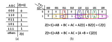 Figure 6. Synthesis of TH23 gate in architecture of [17-20]: a) Operations table; b) Next-state equation.
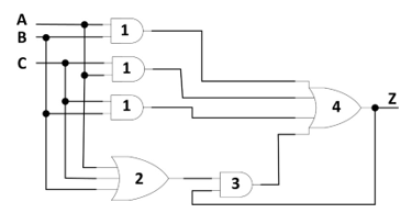 Figure 7. FM architecture of [17-20]: netlist of TH23 gate.
2.2. Synthesizing standard RS as NCL gate
The synthesis of NCL THmn gates in standard RS architecture based on [15] (see Figure 8) extracts the FSET and FRESET functions as shown in [3]. For NCL gate THmn the FSET function is the Z function itself, but using its complemented products. The FRESET function can be described by an OR gate of fan-in=n, which detects when the n input signals are set to zero. The TH23 gate will be used to illustrate method and architecture. Since the Z function of TH23 gate is AB + AC + BC, then the FSET function is {(AB)’, (BC)’, (BC)’}. Figure 9b shows the FSET function extraction, starting from the operations table and Myers’ [3] method, as well as the extraction of FRESET function. The logic circuit of TH23 gate is shown in Figure 10.
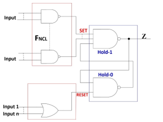 Figure 8. Standard RS architecture in the FM for NCL gates.
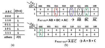 Figure 9. Synthesis of TH23 gate in the standard RS architecture: a) Operations table; b) Fset and Freset equations.
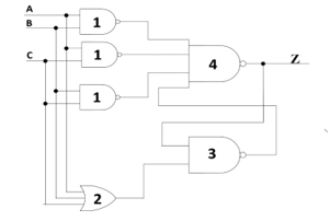 Figure 10. Standard RS architecture: netlist of TH23.
2.3. Synthesizing modified RS as NCL gates
The implementation of THmn NCL gates in modified RS architecture was proposed in [1] (see Figure 11). It follows conventional extraction of the FSET and FRESET functions as shown in section 2.2, but products of FSET are not complemented. To illustrate the method and architecture, it is used the same TH23 gate. Equation 1 describes the architecture of [1] that is composed by the FNCL-SET and FNCL-RESET equations. Equations 2 and 3 are extracted using the same procedure described in Figure 9, where FNCL-RESET is complemented. Finally, equation 4 is obtained from equations 2 and 3, which is the next-state equation of the TH23 gate. Figure 12 shows the logic circuit of TH23 gate in this architecture.
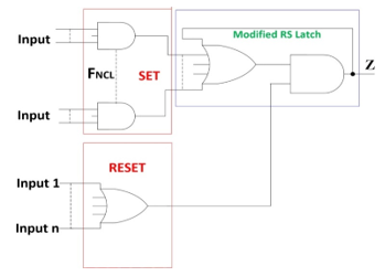 Figure 11. Modified RS architecture in the FM for NCL gates of [1].
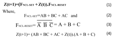
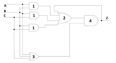 Figure 12. Modified RS architecture: netlist of TH23 gate.
3. QDI Boolean Function: Concepts
Boolean functions for QDI are called function blocks (QDI_FB) and they are synthesized in DI codes. There are different DI codes and in this paper, we adopted the dual-rail coding [32]. The QDI_FB circuits that will be synthesized operate behaving according to the 4-phases handshake protocol [4]. In the dual-rail code, each variable is encoded with two bits. For the variable A, we have A1A0=00 (null – space), A1A0=01 (data 0), A1A0=10 (data 1) and A1A0=11 (never occurs). The DI codes generate the operation completion signal without need of a delay element and with a relatively simple circuit.
3.1. Boolean function: QDI condition
The delay-insensitive (DI) combinational circuits are subject to hazard. Hazardous circuit means that there is a potential for glitches to occur, so it may lead to malfunctioning. The hazard manifests in DI circuits through gate orphan and wire orphan, i.e., a circuit is DI if it is free of gate orphan and wire orphan.
Definition 1 – Gate orphan: Being a function block called FB; it has a gate orphan if a sequence of signal transitions across a path of one or more gates is not recognized by a transition signal on any primary output.
Definition 2 – Wire orphan: Being a function block called FB; it has a wire orphan if the signal transition on a line is not recognized by a transition signal on any primary output.
Since QDI combinatorial circuits satisfy the isochronic fork assumption then these are free of wire orphan, so the combinatorial circuit is QDI if it is free of gate orphan. Figure 13a shows a circuit where input signal transition acts on gates 1 and 2, but it is not recognized by the output signal related to gate 2, so we have a wire orphan. Figure 13b shows the transition of two input signals that activate the OR gate, but it is not recognized by the output signal related to gate 3, so there is a gate orphan, which means that the circuit is not QDI.
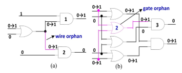 Figure 13. Hazard delay-insensitive of [14]: a) wire orphan; b) gate orphan.
3.2. QDI Boolean function: interaction with environment
A function block for a QDI circuit is required to indicate when its cycles of operations NULL and Valid Data are completed. Hence, by observing the function block outputs, the environment must be able to determine when all input and internal signals have settled. This behavior is shown by a property called indicatability [30, 31]: the signal transition a is indicated by b since the occurrence of b indicates that a has already occurred. We say that a circuit is indicating if it possesses the indicatability property [30, 31]. The indicatability property ensures that no circuitry outruns a signal which changes slowly. Furthermore, the presence of hazards in an indicating circuit is excluded [30, 31].
 Figure 14. Input-output timing behavior of QDI circuits: a) input arrival; b) strong-indication; c) weak-indication; d) early-indication.
The indicatability property tells you how robust the circuit is in aspect of timing analysis and freedom of orphan. Figure 14 shows the three types of interaction where strong indication is the most robust and, early indication (output) is the least robust. Strong indication means that the output signal transitions will only occur when all input signals are NULL (space processing) or all input signals are valid (data processing). Weak indication means that some transition of the output signal may occur without all input signals being NULL or valid, but for the last transition of the output signal, all input signals are NULL or valid. Early indication means that for all transition of output signals be NULL or valid, the input signals are not necessarily NULL or valid.
If the function block does not indicate inputs on the outputs, it is necessary to add circuitry to ensure correct QDI operation. The inputs are indicated through circuitry with a single Boolean output, whose only purpose is to indicate transitions on the input variables. This circuit is called a status detector. The output from status detector together to the output from function block is used by the environment to ensure correct QDI operation [30, 31].
3.3. Timing analysis
The basic assumption behind QDI circuits is that gates and wires have unbounded unknown delays; the only timing assumption permitted is the isochronic fork – whenever a wire forks to two destinations or more, delays on the forks are approximately equal [3, 4]. In contrast, our approach assumes that the delay of gates and wires are bounded by given time intervals:
(TpMIN-G, TpMAX-G) for a gate and (TpMIN-W, TpMAX-W) for a wire, these intervals represent the lower- and upper-bound delays for propagating an input change to the output in a gate. These delays can either be obtained from standard-cell library characterizations or they can represent the theoretical limits of parametric variation. For simplicity, we despised the delays in wires and we will analyze the three architectures presented in Figures. 5, 8 and 11.
I. NCL gates as Huffman machine
By making a timing analysis of the circuit of Figure 7, we have the inequality 5 that reports QDI constraint of the circuit. Analyzing (5), Tp is the propagation time of a gate, and it can be anywhere in range {minimum, maximum}. If the inequality is not satisfied, we will have glitches in output which occur in reason of the fundamental mode violation. As an example, assuming that A and B go from 0→1 and C=0, Z goes from 0→1 and immediately, A goes from 1→0. So Z can vary 1→0→1→0 if (5) is not satisfied. This case shows clearly that to the TH23 gate to operate correctly it must obey to the fundamental mode, so it is not QDI.
2xTpMIN-AND1 + TpMIN-OR4 > TpMAX-OR2 + TpMAX-AND3 (5)
II. NCL gates as standard RS
The inequality 6 shows QDI constraint of Figure 10 circuit. By analyzing (6), we can have glitches if the inequality is not satisfied. As shown in the architecture of Figure 5, glitch in the output occurs because of fundamental mode violation, so the TH23 gate is not QDI.
2xTpMIN-NAND1+TpMIN-NAND4> TpMAX-OR2 + TpMAX-NAND3 (6)
III. NCL gates as modified RS
The inequality 7 shows QDI constraint of Figure 12 circuit. By analyzing (7), we can have glitches if the inequality is not satisfied, for the processing of valid data → null data → valid data. As shown in the architecture of Figure 8, the glitch in the output occurs because of fundamental mode violation, so the TH23 gate is not QDI.
2xTpMIN-OR3 + TpMIN-AND4> TpMAX-AND1 + TpMAX-OR2 (7)
4. Synthesis of QDI NCL Gates: Proposed
The design of NCL THmn gates, in case TH23, THand0, TH24comp and TH34w3, will illustrate the approach in the proposed architecture of Figure 4. For THand0 gate, the function is Z = AB + BC + AD while for TH24comp gate, the function is Z = AC + AD + BC + BD. For TH34w3 gate, the function is Z = A + BCD.
4.1. Synthesis of NCL gates
The implementation of proposed THmn NCL gates follows the conventional extraction of FSET and FRESET functions, as shown in section B. FSET function is the NCL gate function itself. FRESET function is the detection of n signals going to zero, therefore being an OR gate with fan-in equaling to n. Figure 15 shows the logic circuit of NCL TH23 gate where FSET = AB + AC + BC and FRESET = A+B+C. Figures 16, 17 and 18 show the THand0, TH24comp and TH34w3 gates in the proposed architecture, respectively.
 Figure 15. Proposed architecture: netlist of TH23 gate.
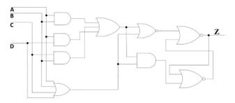 Figure 16. Proposed architecture: THand0 gate.
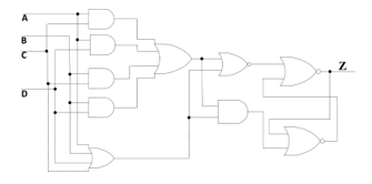 Figure 17. Proposed architecture: TH24comp gate.
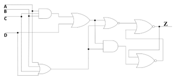 Figure 18. Proposed architecture: TH34w3 gate.
4.2. Timing analysis of proposed NCL gates
Performing the timing analysis in Figure15 circuit, we have that assuming A and B going from 0→1 and C=0, the AND1AB gate goes 0→1, OR3 gate goes 0→1 and NOR4 gate goes 1→0; concurrently the OR2 gate goes 0→1, then AND5 gate goes 0→1 and NOR7 gate 1→0 which the Z output goes 0→1. Immediately, A and B goes from 1→0, so AND1AB goes 1→0, OR3 gate goes 1→0; concurrently OR2 gate goes 1→0 and NOR4 gate goes 0→1 which Z output goes 1→0. For the AND5 gate being QDI, it may be in processing, i.e., still with the value of 1 and consequently, the gate NOR7 with a value of 0, which means that inputs cannot be activated immediately (I/O_M mode). This situation can be measured as shown by inequality 8.
By analyzing (8), we can have glitches if the inequality is not satisfied, for Figure 15 circuit. Since the condition of inequality 8 is robust, i.e., five terms with minimum delay against two maximum delay terms, we can say that it satisfies any DSM-CMOS technology, even if operating at subthreshold voltage, therefore we can accept this gate operating in I/O_M mode as being QDI.
2xTpMIN-NOR4 + TpMIN-NOR6 + TpMIN-NAND1 + TpMIN-NOR3 >
TpMAX-AND5 + TpMAX-NOR7 (8)
4.3. Dual-rail NCL Gates
A minimized two-level F function to be implemented as QDI is initially decomposed in basic gates only of fan-in = 2. The basic gates that can be used are: NOT, AND2, OR2, XOR, XNOR, NAND2, NOR2 and AOI4. The seven gates of fan-in = 2 are extended to dual-rail. The dual-rail NOT gate is simply two swapped wires. Each dual-rail basic gate is implemented as NCL gate generating a library of seven dual-rail NCL gates.
The expansion uses the dual-rail code where each signal is encoded in two wires. Figure 19a shows the dual-rail code table for signal a(a1, a0). For a1a0 = 00, it is NULL which means absence of data; for a1a0 = 01 and a1a0 = 10 mean values 0 and 1, respectively. Figure 19b shows the symbol of dual-rail AND4 gate that is implemented from NCL gates knowing that the function FAND2 = ab and the inverse function is F’AND2 = a’b’ + a’b + ab’.
Generating the dual-rail expansion, we have: from FAND2, we obtain F1AND2 = a1b1 and from the inverter F’AND2, we obtain F0AND2 = a0b0 + a0b1 + a1b0. The F1AND2 function is mapped to the NCL TH22 gate and the F0AND2 function is mapped to NCL THand0 gate. Figure 19c shows the generated THDR-AND2 gate. Using the same procedure, we can build other THDR-X gates. Figures 20, 21 and 22 show the gates THDR-OR2, THDR-XOR and THDR-AOI4, respectively.
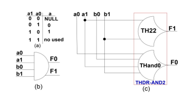 Figure 19. Dual-rail AND Gate: a) Symbol; b) NCL implementation.
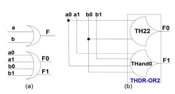 Figure 20. Dual-rail OR gate: a) Symbol; b) NCL implementation.
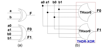 Figure 21. Dual-rail XOR gate: a) Symbol; b) NCL implementation.
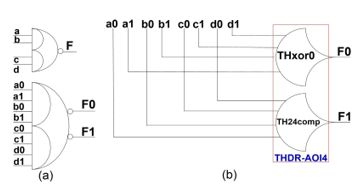 Figure 22. Dual-rail AOI gate: a) Symbol; b) NCL implementation.
Theorem 1. Let the dual-rail NCL gates (THDR-X) synthesized in the proposed approach in section C and implemented in architecture shown in Figure 4. These circuits interact with strong indication.
Proof: Assume all input and output signals are initially in NULL state, since the two functions that make up the THDR-X gate are canonical, then during valid data cycles, every implicant when activated, all input signals acting on the THDR-X must be valid. Since the two TH-X gates contain the reset functions and form the THDR-X gate, then during the NULL cycles all signals that act on the THDR-X gate must go to NULL, therefore the circuit operates with strong indication.
4.4. Proposed Approach for NCL Circuits synthesis
The method starts from a minimized two-level function F_IT (independent of technology) and it follows three steps:
- Performance of the conventional technology mapping of the F_IT function using only a basic gates library: The mapping is performed, for example, by the SIS [22] tool in the target library [NOT, AND2, OR2, XOR, XNOR, NAND2, NOR2 and AOI4] and to obtain the F_DT function (technology dependent).
- Performance of the dual-rail extension of each gate of the F-DT function obtaining the F-DT-dual-rail.
- Performance of the trivial mapping of the F-DT-dual-rail using a target library of seven dual-rail NCL gates.
To illustrate the approach, we have the minimized function F(A,B,C,D) = AÅB + CD mapped to a conventional library. The approach performs a mapping that generates for each term of the F function a dual-rail NCL gate and it ends with the NCL dual-rail OR gate. Figure 23 shows mapping to the NCL function and Figure 24 shows mapping of the NCL function to dual-rail NCL. Figure 25 shows implementations in proposed architecture of the NCL gates THxor0, THand0 and TH22, used in the function mapping.
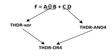 Figure 23. Proposed approach: mapping of NCL gates of F function.
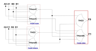 Figure 24. Dual-rail F function: NCL gates.
Theorem 2. Let a dual-rail minimized two-level F function synthesized in the proposed approach of section D with NCL gates THDRmn of section C. This circuit is QDI with constraint of inequality 8 and it interacts with strong indication.
Proof: Assume all the input and output signals of the dual-rail F function are initially in NULL state. The dual-rail F function is free of wire orphan due to isochronic fork assumption. During valid data cycles, the dual-rail F function is free of gate orphan, because of each term of F being associated with a THDR-X gate and there is freedom of gate orphan, with the constraint of inequality 8. As each THDR-X gate operates with strong indication, then the dual-rail function F operates with strong indication, because all terms of the dual-rail F function are activated, either true or false, so all input signals must be valid . For the NULL cycles, the analysis is analogous.
 Figure 25. Proposed architectures: a) THxor0 gate; b) TH22 gate.
5. Case Study
In this section we illustrate an approach for the synthesis of NCL circuits. We use an example found in [33] that is a one-bit ALU (Arithmetic Logic Unit) which can be generalized to N bits by using the concept of carry propagation. The ALU is based on the 8-bit ALU of 74181 TTL integrated circuit. Figure 26 shows the table operations with 12 operations being partitioned into three blocks (selection signals M and C0). Figure 27 shows the first step of the approach that is conventional technology mapping generating the multi-level one-bit ALU. The second step transforms the basic gates (single-rail) into dual-rail gates, as shown in Figure 28. The obtained ALU circuit is implemented with XOR, AND2 and OR2 dual-rail gates. The third step performs the trivial mapping of each dual-rail gate into dual-rail NCL gates (THDR-X), as shown in Figure 24, thereby generating the final NCL circuit, as shown in Figure 29.
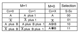 Figure 26. Table of Operations of the ALU presented in [33]
6. Simulation and Results
The design of six benchmarks in two different architectures, in case NCL_D [25], and proposal were synthesized. We also design three NCL gates in four different architectures. These designs were made in structural VHDL, compiled and simulated post-layout in ALTERA tool, Quartus II software, version 9.0, Cyclone III family, in EP3C16F484C6 [34] device.
6.1. Simulations
The simulation post-layout of TH23 NCL gate is shown in Figure 30. Different operations were tested and the waveforms of Figure 30 show its correctness, following the ones shown in operation table of Figure 6a.
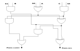 Figure 27. Logic Circuit: Multi-level 1-bit ALU [33].
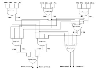 Figure 28. Dual-rail ALU: 1-bit Basic cell.
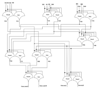 Figure 29. NCL ALU: 1-bit Basic cell.
Figure 31 shows the simulation of NCL ALU. The waveforms show correct results for different tested operations, following the ones shown in operation table of Figure 26. Figure 31 also shows that there are no glitches in the output signal, when compared with the conventional ALU that shows some glitches. The sequence of operations follows the 4-phase handshake protocol, therefore in the timing diagram when all the signals are zero means data absence.
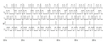 Figure 30. Post-layout simulation: TH23 gate.
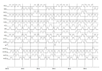 Figure 31. Post-layout simulation: 1 bit ALU.
6.2. Results
Table I shows the results obtained for: area, where only LUTs were used; dynamic power; and latency. Table I is related to the implementation in four architectures of the NCL gate TH23. Analyzing the results of Table I, we have: comparing area in number of LUTs, the proposed architecture, although requiring two LUTs, shows a greater robustness to operate in I/O mode. The proposed architecture obtained an average reduction of 18.6% in latency time when compared with the other three architectures; also obtained an average reduction of 74.0% in dynamic power consumption.
Table II shows the results of six QDI examples design which are: AND of fan-in = 4; detector of prime numbers of 4 bits; detector of odd numbers of 4 bits; full adder of 1 bit; multiplier of 2 bits; ALU of 1 bit of [21]. These examples were synthesized in the NCL_D [25] approach using DIMS components [12] and in the proposed architecture of Figure 4 being both architectures of the type strong indication. The results of six examples in Table II are: number of LUTs; latency time; and the dynamic and static power. Analyzing Table II and comparing the proposal with and NCL_D, we have an average reduction of 13.6% in area (number of LUTs) and 13.7% in static power. There was an average penalty of 4.6% and 32.5% in latency time and dynamic power, respectively.
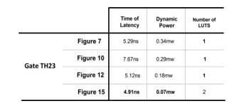 Table 1. Results of th23 ncl gate in differents architetures
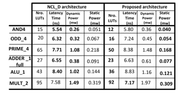 Table 2. Results of the six examples
7. Conclusions
When comparing the implementation of TH23 NCL gate stated in Table I, our approach clearly shows advantages in terms of latency and power consumption, despite the penalty in area. Therefore, when designs are bounded by achieving the best performance or lower power consumption our approach is advantageous, but for designs bounded by area constraints it is not the best option. Regarding Table II, when it comes to a complete QDI circuit our approach is superior in terms of area.
As a way to increase robustness to FM violation in the NCL gates architectures based in basic gates, it is possible to insert delay elementes in paths that are sensitive to FM mode. This strategy though, has three problems: a) delay elements are not easy to add in FPGAs; b) delay elements degrade the reliability and testability of circuits; c) insertion of delay elements tends to decrease performance and increase power consumption. Thus our approach is more robust because delay elements are not needed.
Due to many different applications requiring robust digital systems in the processing or in data security, an interesting solution shows to be robust components using in their synthesis. In this paper, we present an approach and architecture to synthesize NCL gates on platforms FPGA and standard-cell VLSI. The proposed architecture based on basic gates implements NCL gates that operate in I/O_M mode and they are QDI with restriction of inequality 8 while other architectures based in basic gates generate NCL gates that operate in FM mode, so they are not QDI. Comparing with other approaches [27-31] which need of an additional signal to satisfy the property of indicatability, our approach does not insert any signal. The proposed NCL gates presents other interesting properties such as high robustness to variations in temperature and to supply voltage, which occurs very often in hostile environments such as in space and in certain areas of military combat. For further works, it is desirable to test the proposed NCL gates considering radiation effects of SEU (Single-Event Upset) in FPGA platform [35, 36].
Conflict of Interest
The authors declare no conflict of interest.
- D. L. Oliveira, O. Verducci, L. Faria, T. Curtinhas, “A novel null convention logic (NCL) gates architecture based on basic gates” in IEEE XXIV International Conference on Electronics, Electrical Engineering and Computing (INTERCON), Cusco, Peru, 2017. https://doi.org/ 10.1109/INTERCON.2017.8079680.
- B. H. Calhoun, et al., “Digital Circuit Design Challenges and Opportunities in the Era of Nanoscale CMOS,” Proc. of the IEEE, Vol. 96, No. 2, pp. 343-365, February 2008. https://doi.org/10.1109/JPROC.2007.911072.
- C. J., Myers, “Asynchronous Circuit Design”, Wiley & Sons, Inc., 2004, 2a edition.
- P. Beerel, R. Ozdag and M. Ferretti, “A Designer’s Guide to Asynchronous VLSI”. Cambridge University Press, p. 337, 2010.
- J. Martin, “Compiling Communication to Delay-Insensitive VLSI Circuits”, Distributed Computing, 1(4), pp.226-234, December 1986. https://doi.org/10.1007/BF01660034.
- J. Martin, “The Limitations to Delay Insensitive in Asynchronous Circuits,” 6th MIT Conference on Advanced Research in VLSI Processes, pp.263-277, 1990. https://doi.org/10.1007/978-1-4612-4476-9_35.
- J. Cortadella, A. Kondratyev, L. Lavagno, and C. Sotiriou, “Coping with the variability of combinational logic delays,” ICCD, pages 505–508, 2004. https://doi.org/10.1109/ICCD.2004.1347969.
- W. Hardt, et. al., “Architecture Level Optimization for Asynchronous IPs”, Proc. 13th Annual IEEE Int. Conf. ASIC/SOC, pp.158-162, 2000. https://doi.org/10.1109/ASIC.2000.880694.
- L. Spadavecchia, “A Network-based Asynchronous Architecture for Cryptographic Devices,” PhD thesis, University of Edinburgh, 2005.
- C. L. Seitz, “System Timing,” in Introduction to VLSI Systems, Addison-Wesley, pp. 218-262, 1980.
- I. David, R. Ginosar, and M. Yoeli, “An Efficient Implementation of Boolean Functions as Self-Timed Circuits,” IEEE Transactions on Computers, Vol. 41, No. 1, pp. 2-10,1992. https://doi.org/10.1109/12.123377.
- J. Sparsø, J. Staunstrup. “Delay Insensitive Multi Ring Structures”, Integration, the VLSI Journal. v15(13), 1993. https://doi.org/10.1016/0167-9260(93)90035-B.
- K. M. Fant and S. A. Brandt. “NULL convention logic: a complete and consistent logic for asynchronous digital circuit synthesis”. In International Conference on Application Specific Systems, Architectures and Processors, pp. 261-273, 1996. https://doi.org/10.1109/ASAP.1996.542821.
- F. A. Parsan and S. C. Smith “CMOS Implementation of Static Threshold Gates with Hysteresis: A New Approach,” In Proceedings of the IFIP/IEEE International Conference on VLSI-SoC, Santa Cruz, CA, USA, 7–10, pp. 41-45, October 2012. https://doi.org/10.1109/VLSI-SoC.2012.7332074.
- F. A. Parsan and S. C. Smith, “CMOS Implementation Comparison of NCL Gates,” In Proceedings of the IEEE International Midwest Symposium on Circuits and Systems, Boise, ID, USA, 5–8 August pp. 394-397, 2012. https://doi.org/10.1109/MWSCAS.2012.6292040.
- S. C. Smith, et al., “Optimization of NULL convention self-timed circuits,” INTEGRATION, the VLSI journal 37, pp.135–165, 2004. https://doi.org/10.1016/j.vlsi.2003.12.004.
- V. Satagopan, et al., “DFT Techniques and Automation for Asynchronous NULL Conventional Logic Circuits,” IEEE Trans. on Very Large Scale Integration (VLSI), vol. 15, no. 10, pp.115-1159, October 2007. https://doi.org/10.1109/TVLSI.2007.903945.
- W. K. Al-Assadi and S. Kakarla, “Testing of Asynchronous NULL Conventional Logic (NCL) Circuits in Synchronous-Based Designs,” 22nd IEEE International Symposium on Defect and Fault Tolerance in VLSI Systems, pp.215-222, 2007. https://doi.org/10.1109/DFT.2007.40.
- W. K. Al-Assadi and S. Kakarla, “Design for Test of Asynchronous NULL Convention Logic (NCL) Circuits,” IEEE International Test Conference, pp.1-8, 2008. https://doi.org/10.1109/TEST.2008.4700611
- L. Duc Tran, et al., “Null Convention Logic (NCL) based Asynchronous Design – Fundamentals and Recent Advances,” International Conference on Recent Advances in Signal Processing, Telecommunications & Computing (SigTelCom), pp.158-163, 2017. https://doi.org/10.1109/SIGTELCOM.2017.7849815.
- S. C. Smith, “Design of an FPGA Logic Element for Implementing Asynchronous NULL Convention Logic Circuits,” IEEE Transactions on Very Large Scale Integration (VLSI) Systems, vol. 15, no. 6, pp. 672-683, June 2007. https://doi.org/10.1109/TVLSI.2007.898726.
- M. M. Kim, et al., “Design Techniques for NCL-based Asynchronous Circuits on Commercial FPGA,” 17th Euromicro Conference on Digital System Design, pp.451-458, 2014. https://doi.org/10.1109/DSD.2014.85.
- T. Chelcea, G. Venkataramani, S. C. Goldstein, “Area Optimizations for Dual-Rail Circuits Using Relative-Timing Analysis,” 13th IEEE International Symposium on Asynchronous Circuits and Systems (ASYNC’07), pp.1-13, 2007. https://doi.org/10.1109/ASYNC.2007.10.
- J. Cheoljoo and S. Nowick. “Technology mapping and cell merger or asynchronous threshold networks,” IEEE Trans. on Computer-Aided Design of Integrated Circ. and Systems, Vol. 27(4), pp. 659-672, 2008. https://doi.org/10.1109/TCAD.2007.911339.
- M. Ligthart, K. Fant, R. Smith, A. Taubin, A. Kondratyev, “Asynchronous design using commercial HDL synthesis tools”, Async’00, pp. 114 – 125, 2000. https://doi.org/10.1109/ASYNC.2000.836983
- A. Kondratyev, K. Lwin, “Design of Asynchronous Circuits Using Synchronous CAD Tools”, IEEE Design and Test of Computers, vol. 19, no. 4, pp. 107-117, 2002. https://doi.org/10.1109/MDT.2002.1018139.
- J. Cortadella, A. Kondratyev, L. Lavagno, and C. Sotiriou, “Coping with the variability of combinational logic delays,” ICCD, pages 505–508, 2004. https://doi.org/10.1109/ICCD.2004.1347969.
- Zhou, Y., Sokolov, D., Yakovlev, A.: ‘Cost-aware synthesis of asynchronous circuits based on partial acknowledgement’. Proc. Int. Conf. Computer-Aided Design, San Jose, USA, November 2006, pp. 158–163. https://doi.org/10.1109/ICCAD.2006.320080.
- Fu-Chiung Cheng and Chi Chen, “Can QDI Combinational Circuits be Implemented without C-elements?,” IEEE 19th International Symposium on Asynchronous Circuits and Systems, PP.134-141, 2013. https://doi.org/10.1109/ASYNC.2013.13.
- P. Balasubramanian, and D.A. Edwards, “Efficient Realization of Strongly Indicating Function Blocks,” IEEE Computer Society Annual Symposium on VLSI, ISVLSI ’08, pp.429-432, 2008. https://doi.org/10.1109/ISVLSI.2008.103.
- P. Balasubramanian, “A Robust Asynchronous Early Output Full Adder,” WSEAS Transactions on Circuits and Systems, Issue 7, Volume 10, pp. 221-230, July 2011.
- T. Verhoeff, ‘Delay-insensitive codes – an overview’, Distrib. Comput, 3, (1), pp. 1–8, 1988. https://doi.org/10.1007/BF01788562.
- H. Taub, “Circuitos Digitais e Microprocessadores”, Portuguese edition, McGraw-Hill, 1982.
- Altera Corporation, 2018, www.altera.com.
- W. Jang and A. Martin, “SEU-tolerant QDI circuits,” in IEEE International Symposium on Asynchronous Circuits and Systems, pp. 156–165, 2005. https://doi.org/10.1109/ASYNC.2005.30.
- D. J. Barnhart, et. al. “Radiation Hardening by Design of Asynchronous Logic for Hostile Environments”, IEEE Journal of Solid-State Circuits, vol. 44, No. 5, pp.1617-1628, May 2009. https://doi.org/10.1109/JSSC.2009.2017005.