Topology, Discontinuities and Dimension Effects on CMOS Rotary Traveling Wave Oscillators
 , Mónico Linares Aranda 2, Luis Hernández Martínez 2, Carlos Sanabria Díaz 2
Adv. Sci. Technol. Eng. Syst. J. 3(4), 260–269 (2018);
 DOI: 10.25046/aj030426
In this article, a new method to extract the RLC parameters from the structure of a Rotating Traveling Wave Oscillator (RTWO) is described. The use of a 3D simulator (EMPRO) allow us to develop a precise analysis of the impact of the topology, the geometrical discontinuities, and the dimensions of the transmission lines, on the performance parameters of the RTWO, i.e. frequency of oscillation and power consumption. The results show that a right angle discontinuity compensation can reduce the power consumption up to 3.34% and, for RTWOs with a frequency range between 11.4 GHz and 11.5 GHZ, narrow transmission lines (as the technology is able) can reduce the power consumption up to 98%. Additionally, it was observed that the topology used affects the performance parameters, as there are more folds and overlaps between metal levels in the RTWO structure, and the frequency increases by 2.9% while the power consumption increases by 10.52%.
1. Introduction
Nowadays, the high and very high-frequency ranges (millimeter range: 10-66Hz, and THz range: 0.1THz10THz) are an object of study due to their promising applications in the military, commercial, communications and medical fields; which include spectroscopy, remote environmental sensing, high-resolution biological imaging, mobile telecommunications, and broadband satellite communications, among others [1, 2, 3]. On the other hand, in the past, only critical circuits, essentially high-precision clock systems, operated at high frequency.
However, this is no longer true at the present highspeed digital design. Many of the signal processors and their interconnections operate and transmit signals at frequencies in the MHz range and even in the GHz range. This is the case of high-performance information systems, which after the current demand of developing faster and faster electronic devices able to perform a wide number of functions (computers, telephones, tablets, and so on), generate the need to increase the operating frequency of the microprocessors to the GHz range with a minimum power consumption. Consequently, the conventional systems of clock generation and/or distribution, commonly used in the current ICs (H-tree, X-tree, mesh, etc.), become obsolete.
The common element used in the previously mentioned applications is the oscillator: a periodic signal generator circuit that operates at the highest frequency in any synchronous system. In communications systems, the clock element is the Voltage Controlled Oscillator (VCO), usually included in the Phase Tie Loop (PTL) and in microprocessor systems. Currently, there is a new resonant oscillator type based on transmission lines. To synchronize signals on CMOS chips, different high-speed resonant oscillator structures have been created: distributed differential oscillators [4], fixed wave oscillators [5], and Rotary Traveling Wave Oscillators (RTWO) [6], among others. From these technologies, the RTWO stands out for its multiple advantages such as high oscillation frequencies, low power consumption, multiphase signals, low jitter, low skew and simple design [7].
The RTWO is an innovative approach which takes advantage of the distributed Inductive and Capacitive (LC) nature of the interconnection lines, present at the CMOS processes used for the manufacture of integrated electronic systems. RTWOs are used for the generation of multi-GHz signals in communication systems, and the generation/distribution of clock signals in high-performance microprocessors [6].
The RTWO generates the oscillations through the LC elements associated with the transmission lines which form the resonant structure. Hence, the operation and performance of an RTWO depend on the physical properties of the materials used, the dimensions of the transmission lines (width W, length l, and thickness T ), the discontinuities of the line (curves, crossings, vias, joints, etc.), and the topological structure used (circular, square, hexagonal, etc.).
Several works have been published concerning the design of the RTWOs. In [11], a rectangular topology was implemented and analytical approaches were used to obtain the RLC parameters. [19, 20] implemented different RTWOs in a 180 nm technology with a frequency range from 2GHz to 12GHz, using a rectangular topology and a 2D electromagnetic simulator to extract the RLC parameters. In [17], RTWOs were designed in a 65nm technology achieving a frequency range from 110 GHz to 152GHz. That work implemented an octagonal topology while the extraction of the RLC parameters was done by means of a 2D electromagnetic simulator. [23] used a 180nm technology with a frequency range from 3GHz to 11GHz, and although the extraction of the RLC parameters was done by a 3D electromagnetic simulator, they segmented the ring to perform the simulation, so they did not take into account many of the effects obtained when the complete ring is simulated.
Most of the mentioned previous works used analytical approximations or 2D simulators for the extraction of the RLC parameters. Since the analytical approximations are not exact and the 2D simulators do not take into account some electromagnetic effects on the ground plane, such as skin effect and proximity effect, the designed RTWO could not oscillate at the desired frequency or, in the worst case, could not oscillate.
In this work, a new design method was developed. A 3D electromagnetic simulator was used to extract the RLC parameters of the RTWO structure, which allows us to perform an accurate analysis of how the frequency of oscillation and power consumption are affected by the dimensions of the RTWO (length, width and gap between the transmission lines), right-angle discontinuities, and the different topologies used in RTWO design. In this way, it is possible to simultaneously analyze the effect of the geometric discontinuities and the topology on the operating parameters of the RTWOs.
2. The RTWO
The Rotatory Traveling Wave Oscillator (RTWO) is a closed loop implemented with a differential transmission line (displaying LC characteristics) with a connected crossing from the inner conductor to the outer
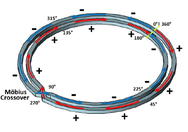 Figure 1: Typical circuit topology of a RTWO.
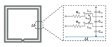 Figure 2: Equivalent electrical circuit of an infinitesimal section of an RTWO.
conductor (Mo¨bius crossing), which causes a reversal in the signal (Figure 1). Oscillation begins with any noise event. If there were no losses, a wave would travel in the ring indefinitely, providing a complete clock cycle every two rotations to the ring (Mo¨bius effect).
To model the electrical behavior of the RTWO resonant circuit, an equivalent electrical circuit of distributed elements (RLC) is used. The effects of the transmission line are modeled by resistance (R11 and R22), self-capacitance (C11 and C22) and selfinductance (L11 and L22), while the magnetic and electrical coupling are modeled by mutual inductance (L12), and mutual capacitance (C12), respectively. The equivalent electrical circuit is shown in Figure 2.
Since there are losses in the conductor due to discontinuities or the dielectric, the signal will be attenuated while it travels through the resonant circuit. Therefore, an amplification stage is required to compensate the losses of the resonant circuit. For the amplification stage, a topology consisting of two inversers antiparallely connected (CCIP) were used. Additionally, the CCIPs block the phase, which causes the odd propagation mode, i.e. a signal in one line will be offset by 180◦ from the signal in the other line. The compensation stage configuration is shown in Figure
The CCIP stages will generate negative resistance (transconductance), which compensates the resistive losses of the resonant circuit. These compensation stages are evenly redistributed throughout the ring.
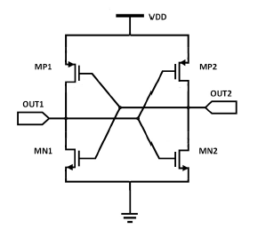 Figure 3: RTWO compensation stage.
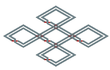 Figure 4: Rotary Oscillator Array (ROA).
2.1. Rotary Oscillator Array (ROA)
Multiple RTWOs can be connected together to form an array of rotating oscillators that distribute a signal to the entire chip. Figure 4 shows a basic structure of a ROA constituted by five RTWO rings connected in a checkerboard topology.
The inner rings and outer rings of the adjacent RT-WOs are physically connected for synchronization purposes [14]. The advantage of implementing a ROA instead of a single RTWO is that a ROA provides more interconnection points, which eliminates the need of using too long interconnections between the synchronous element and the oscillator. The decrease in interconnection length provides the reduction in signal delay caused by the effects of high-frequency interconnections.
2.2. RTWO design parameters
Two of the main design parameters of a RTWO are power consumption and frequency of oscillation, which will be described in the following sections.
2.2.1. Power consumption
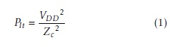
The power consumption of the RTWO is the sum of the contribution of the resonant circuit and the compensation stages, where the power dissipated by the resonant circuit Plt can be calculated by Equation 1:
 The power consumption of the compensation stage PCCIP is divided into three components: the static power consumption, which is negligible; the dynamic power, which is recirculated and converted into energy for the resonant circuit; and the short circuit power, which cannot be ignored and is consumed when both NMOS and PMOS transistors are switched on [15]. PCCIP is expressed by Equation 2 as:
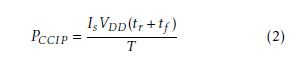 Where Is is the saturation current, tr is the signal rise time, tf is the signal fall time and T is the signal period.
2.2.2. Frequency of oscillation
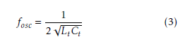
The frequency of oscillation fosc is a factor of the total capacitance Ct and the total inductance Lt, as is expressed in Equation 3.
 Lt is just related with the differential transmission line, while Ct depends on Equation 4. Clt is the capacitance of the differential transmission line, Ccomp is the capacitance of the compensation stage and Cload is the load capacitance.
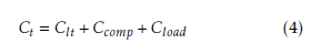 As is seen from Equations 3 and 4, fosc will strongly depend on the geometry of the RTWO and the compensation stage.
2.3. RTWO structure and manufacture
The RTWO of the present work was built using a 180 nm mixed-mode UMC manufacturing technology, which uses a single level of polysilicon and 6 levels of metal (1P6M), P-type substrate, and RFCMOS. The structure was made of aluminum at level 6, with the Mo¨bius crossing at level 5. Figure 5 shows a schematic of the technology used. The main physical and electrical parameters of the RTWO are shown in Table 1.
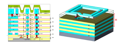 Figure 5: (a) Cross-section view of the UMC 180 nm RFCMOS manufacturing technology, (b) 3D structure of the RTWO.
Table 1: UMC 180 nm CMOS manufacturing process parameters, and RTWO geometrical features.
| Parameter | Symbol | Value |
| Conductivity (S/m) | σ | 37×106 |
| Material permitivity | εr | 3.8 |
| Vacuum permitivity (F/m) | ε0 | 8.854×10¹² |
| Vacuum permeability (H/m) | µ0 | 4π ×10−7 |
| Line thickness (µm) | T | 2.06 |
| Oxide thickness (µm) | H | 6.52 |
| Line length (µm) | l | 1000 |
2.4. Geometrical discontinuities
The abrupt changes in the conductor geometry of the transmission line cause geometrical discontinuities. Consequently, the electric and magnetic field distributions are modified near the discontinuity when highfrequency signals are transmitted through them.
In RTWOs design, right-angled corners origin a build-up of load particularly on the outside of the corner, which causes capacitance overload. Similarly, the interruption of the current flow produces inductance overload [8, 9]. Since the excess of capacitance and inductance change the frequency of oscillation and the power consumption of the RTWO, it is necessary to use a compensation technique for this type of geometrical discontinuity.
There are different useful techniques to compensate the excess of capacitance and inductance caused by 90◦ corners. These techniques remove some of the metal from the corners. Figure 6 shows the full-wave results from a geometrical discontinuity simulation. The current density is best redistributed by a 45◦ chamfer, 1 side [16]. Therefore, the less load build-up at the corners decreases the capacitance, compared to a right angle corner.
2.5. Topologies
In RTWO design, several topologies of different shapes are known, such as circular, hexagonal, octagonal, and square with different number of crossings. These topologies have been applied in [10, 17, 18, 21]. However, there is no analysis joining the effect of the diffrent discontinuities on the answer of an RTWO. In RTWO design, the dimensions of the oscillator, the design of the compensation stage, the geometric discontinuities, and the topology used for the oscillator, have a high impact on the inductance and capacitance of the differential transmission lines from which the oscillator is built. As consequence, they affect the oscillation frequency and the power consumption of the RTWO.
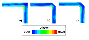 Figure 6: Current distribution on transmission line using mitered techniques: (a) Right angle bend (no mitered), (b) 45◦ chamfer – 1 side, (c) 45◦ bend – 2 sides.
3. Methodology
In order to include the effects of the geometrical discontinuities, in [19] and [23] the transmission lines of the rotating ring were divided into uniform segments. However, the union of the different segments presents differences in contrast with the superposition of the effects by segments. Both technique differ from the simulation of a complete ring [22]. Thus, to minimize the discrepancies and to consider the greatest number of electromagnetic effects in the structure of a RTWO, the methodology used in this work includes the simulation of the full ring.
Different software tools were used to simulate the RTWO due to the fact that the 3D electromagnetic simulator used (EMPRO) only extracts the S-parameters from the full-wave simulation. Then, it requires the use of an additional software to calculate the parameters of the RTWO through the S-parameters (MATLAB in this work), and another one to simulate the electrical circuit of the RTWO (HSPICE). Therefore, in this work the first step was to use EMPRO to develop the 3D geometrical structure of the RTWO. Then, a full-wave simulation was performed by means of the Finite Element Method (FEM). The resulting S-parameters from the simulation were exported to MATLAB. With MATLAB, the RLC parameters, the transistor size of the compensation stage, the power consumption and the oscillation frequency by analytical approaches were calculated. Finally, HSPICE was used to implement the RTWO considering the RLC parameters of the resonant circuit and the compensation stage, simulating the circuit of the distributed elements of the resonant circuit and the compensation stages of the RTWO.
At first, a working frequency range from 11 to 12 GHz was defined. In the simulations of [22], it was determined that with a length of 1000µm, the frequency of oscillation range required was obtained. Therefore, different simulations of the RTWO were carried out varying the width W, the separation between the transmission lines S, and the topology of the RTWO, to observe the impact of these factors over the oscillation frequency and the power consumption. In the simulations developed with HSPICE, eight uniformly distributed amplification stages were used.
4. Effect of W and S on fosc and Pt
All the electrical properties of the interconnections are due to the arrangement of the conductors and dielectrics and the way they interact with the electrical and magnetic fields of the signals. The total resistance of the interconnections depends on the signal strip and the return plane; both resistors depend on the geometry of the conductors and the current distribution in them. The inductance is also composed of two terms, the first related to the inductance inside the conductors and the second term, called external inductance, produced in the proximities of the conductors. Both inductances, as well as the resistance, depend on the current distribution in the conductors. On the other hand, the value of the capacitance depends on the distribution of the charge on the surface of the conductors.
As it was seen, inductance, resistance and capacitance in the interconnections, depend strongly on their geometry. Since the resonator circuit of the RTWO is built by the interconnections of the integrated circuits, and the frequency of oscillation depends on the capacitive and inductive effects of the interconnections, the impact of the width of the interconnections on the frequency of oscillation and the power consumption of the RTWO must be analyzed. Therefore in this work, several simulations were performed considering W in the range of 5 µm to 25 µm. Moreover, the value of S was set at the minimum value of W, in this case, 5 µm.
Figure 7 shows the variation of the total inductance Lt and the total capacitance Ct for the different values of W. As W increases, the cross-sectional area over which the current is distributed increases, so the total number of magnetic field line loops decreases and, therefore, Lt decreases. When increasing the size by W, the transconductance gm required to compensate the losses must increase, so larger transistors are required and, as consecuence, Ccomp increases. In the same way, considering the analogy of a parallel plate capacitor, when increasing the width of the line, the capacitance Clt increases. The increment of both capacitances (Ccomp and Clt) produce the increment of the total capacitance.
Figure 8 shows the variation of the characteristic impedance Zc and the resistance R when varying W. In this case, it can be seen that both parameters decrease with the increase of W because there is a larger crosssection where the current flows through the transmission line. Figure 9 shows how the frequency of oscillation and power consumption varies by increasing W. The low dependency of fosc to W is due to the fact that the increase of Ct is compensated by the decrease of Lt (Figure 7).
Setting the values of l=1000 µm and W=5 µm, another parameter that can be varied is the separation between the transmission lines S. In this case, values from 5 µm to 15 µm were taken for S. Figure 10 shows the variation of Lt and Ct depending on the different values of S.
Due to the separation of the transmission lines, a smaller number of magnetic field lines are annulled, which causes the increase of the mutual inductance and therefore the increase of Lt. On the other hand, as the transmission lines are separated, fewer losses are required to be compensated for, so the size of the transistors decreases and Ct decreases. Figure 11 shows the variation of R and Zc depending on the different values of S. It can be seen from the graph that both R and Zc have little dependence on the separation of the transmission lines.
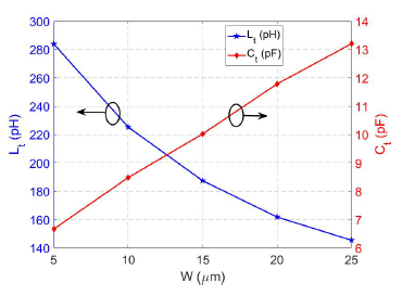 Figure 7: Variation of Lt and Ct when increasing W.
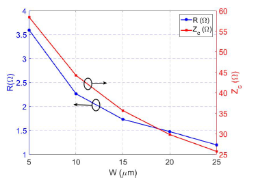 Figure 8: Variation of R and Zc when increasing W.
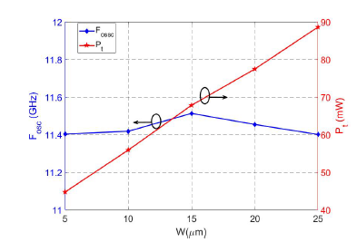 Figure 9: Variation of fosc and Pt when increasing W.
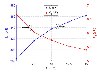 Figure 10: Variation of Lt and Ct when increasing S.
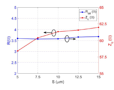 Figure 11: Variation of R and Zc when increasing S.
Finally, Figure 12 shows that fosc remains approximately constant. On the other hand, the power consumption Pt decreases when separating the transmission lines, due to the decrease of the power consumption of the compensation stage.
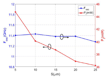 Figure 12: Variation of fosc and Pt when increasing S.
5. Discontinuities compensation effect in squared topology
Prior to the simulation of the different RTWO topologies, the squared RTWO design was optimized by applying two mitered techniques: 45◦ miter – 1 side, and 45◦ miter – 2 sides (Figure 6). Three layouts were developed using the squared topology with a Mo¨bius crossing, by means of the Mentor Graphics Design Editor (Figure 6a). In Layout 1 no mitered was implemented, but in Layout 2 the 45◦ mitered corner – 1 side was implemented, and in Layout 3 the 45◦ mitered corner – 2 sides. For the hexagonal and octagonal layouts, any mitered technique was applied. The performance parameters of the oscillators applying the different mitered techniques are shown in Table 2. It is worth to mention that Layout 4 corresponds to the squared topology of the RTWO built directly with the EMPro electromagnetic simulator, and not with Mentor Graphics, but for ease, it is also included.
Table 2: RTWO performance parameters using different mitered techniques.
| Layout | Fosc(GHz) | Pt (mW) |
| 1 | 11.66 | 41.18 |
| 2 | 11.82 | 39.28 |
| 3 | 12.07 | 37.74 |
| 4 | 11.43 | 40.12 |
From Table 2 is inferred that the 45◦ mitered on both sides of the line (Layout 3), is the most effective mitered technique because it allows to the RTWO having the highest oscillation frequency, in agreement with [16], due to its less capacitance and total inductance variation. In the same way, when comparing values of extracted capacitance, there is a variation of 5% in the total capacitance where EMPro is used directly (Layout 4) and when the RTWO layout is done in Mentor Graphics (Layout 3). This variation is due to the fact that in the layout from Mentor Graphics several vias (small contacts between the different metals of the technology) were used to connect the 5th and 6th levels of metal, while in Layout 4 only one single contact is used, which is unsuitable for real integrated circuits.
6. Topology effect
Figure 13 shows the total variation of the resistance, inductance, and capacitance for the different topologies of the RTWO analyzed. As is shown, the total capacitance increases since there are more crossings in the metal 5 (see topologies in Figures 14d to 14f). This effect is due to the increase in capacitance coming from the crossing. Figure 14(b) shows how the crossing in metal 5 (topologies 4, 5 and 6) increase resistance due to the smaller thickness of the metal 5 in contrast with metal 6. Therefore, the cross-section through which the current flows is lower causes an increase in the resistance.
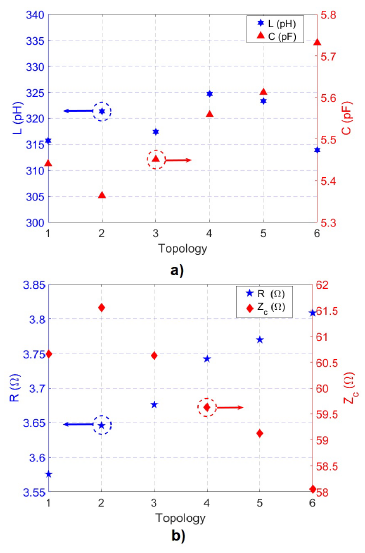 Figure 13: Electrical parameters of the different topologies: Resistance (R), Inductance (L), Impedance (Zc) and Capacitance (C).
Table 3 shows the performance parameters of the RTWO using different topologies. In this table, two crossing types are identified: one where metal levels 5 and 6 intersect diagonally (Mo¨bius crossing), and the other one where metal levels 5 and 6 intersect orthogonally (simple crossing). It is observed that the oscillation frequency between oscillators having only one metal crossing (topologies 1, 2 and 3) is approximately the same; whereas if the number of crossings in metal 5 increases, the oscillation frequency decreases due to the increase of the inductance and the capacitance in the crossings. On the other hand, the power consumption increases as the number of metal 5 crossings increase (topologies 4, 5, and 6), due to the increase of the resistance and the reduction of the characteristic impedance.
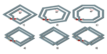 Figure 14: RTWO topologies analyzed: 1) Square with 1 Mo¨bius crossing, 2) Hexagonal with 1 Mo¨bius crossing, 3) Octagonal with 1 Mo¨bius crossing, 4) Square with 2 crossings and 1 Mo¨bius crossing, 5) Square with 3 crossings, 6) Square with 4 crossings and 1 Mo¨bius crossing.
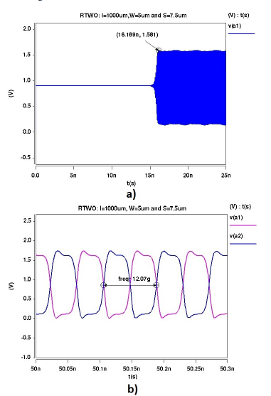 Figure 15: Waveforms of the RTWO oscillator: a) Beginning of the oscillation, b) oscillation of stable complementary nodes.
Table 3: RTWO performance parameters using diferent topologies.
| Topology | Fosc(GHz) | Pt (mW) |
| 1 (Squared-1 Mo¨bius) | 12.051 | 37.44 |
| 2 (Hexagonal-1 Mo¨bius) | 11.972 | 39.00 |
| 3 (Octagonal-1 Mo¨bius) | 11.937 | 39.67 |
| 4 (Squared-2 crossings-1 Mo¨bius) | 11.706 | 40.40 |
| 5 (Squared-3 crossings) | 11.741 | 39.85 |
| 6 (Squared-4 crossings-1 Mo¨bius) | 11.701 | 42.18 |
Figure 15 shows the waveforms of the RTWO. In Figure 15a, is observed that, after 16.189 ns, the RTWO starts to oscillate in a stable form to a frequency of 12.07 GHz with an amplitude of 1.581 V. Figure 15b shows how the waveform of a node is offset by 180◦ from its complementary node. To observe the band nature of RTWO, the spectrum was observed over a span of 100GHz. Figure 16 shows the results of this simulation.
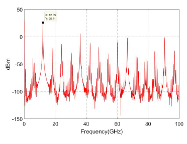 Figure 16: Typical power spectrum-wide band.
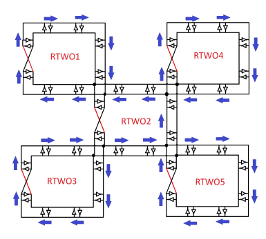 Figure 17: Diagram of the simulated ROA.
7. Design of an ROA
After designing a RTWO, an array of RTWO oscillators was made. In this case, a checkerboard configuration was used in which five RTWOs were connected (Figure 17). Each of the RTWOs is in phase with the others at the connection node. The advantage of a ROA is that multiphase signals can be obtained anywhere in the integrated circuit by reducing the skew and jitter of the signal.
The signal of each of the RTWOs of the ROA is shown in the Figure 18. In this case, only the signal of the external nodes of every RTWO is shown. It can be seen that the signals travel in clockwise direction, while in the middle RTWO (RTWO2) they travel in the opposite direction. Similarly, as the signal passes from one compensation stage to another, the signal is offset. For this case, the offset is given by Equation 5:
![]() Nevertheless, if small oscillation frequencies are desired, they must be made with maneuverable lengths so that Lt and Clt increase their value and therefore the oscillation frequency decreases. This is a disadvantage in the design of RTWOs and ROAs because they will consume a larger area on the chip. Another way to decrease the frequency of oscillation is to be able to increase Ccomp, which can be achieved by making larger transistors for the compensation stage. The disadvantage is that having very large transistors increases the power consumption, therefore there is a strong compromise between the area of the chip and the power consumption in low frequency RTWOs.
Nevertheless, if small oscillation frequencies are desired, they must be made with maneuverable lengths so that Lt and Clt increase their value and therefore the oscillation frequency decreases. This is a disadvantage in the design of RTWOs and ROAs because they will consume a larger area on the chip. Another way to decrease the frequency of oscillation is to be able to increase Ccomp, which can be achieved by making larger transistors for the compensation stage. The disadvantage is that having very large transistors increases the power consumption, therefore there is a strong compromise between the area of the chip and the power consumption in low frequency RTWOs.
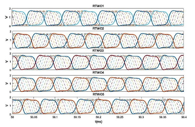 Figure 18: Simulated output waveforms.
8. RTWO performance comparison against existing works
In order to show the efficiency of the designed method applied at the present work, a comparison was made with two published methodologies: the methods of Chen et al. [11] and Aidoo et al. [15]. Chen et al. used analytical approximations in the determination of the electrical parameters R, L and C of the RTWO, including different RTWOs at different frequencies simulated in HSPICE with parameter values of a technology 0.18µm SMIC and a 1.8 V power supply. In contrast, Aidoo et al. divided the RTWO structure into segments with equal dimensions while the parasite parameters were extracted from every segment using a 2D simulator. By this method of bonding segments, Aidoo et al. designed and manufactured different RTWOs using an IBM 0.18µm CMOS technology. Using as reference the RTWO manufactured by
Aidoo et al. at the present work (which oscillates up to
12.2 GHz), two RTWOs were designed with the same ring dimensions as well as of its compensators, but using 8 compensation stages for the design 1, and 28 for the design 2. Later, both the method used by Chen et al. and the one proposed in this work, were applied to extract the parasite parameters from the RTWO. The specifications of the different designs are shown in Table 4.
Since the comparison made in Table 4 considers RTWOs designed by parameters of different technological processes, this might not be a good comparison. In order to improve the comparison, two RTWOs were designed using the same technology (UMC 180 nm RFCMOS): one of them applying the method of Aiddo et al. and another one applying the method proposed in this work. Table 5 shows a comparison of the parasite parameters variations (R, L and C), the size of the transistors, the oscillation frequency and the amplitude of both designs. Km represents the magnetic coupling coefficient of the ring differential line used to develop the electrical simulation in HSPICE. Wp and Wn are the dimensions of the transistors of the compensating circuit.
Table 4: RTWOs specifications using different manufacturing technologies (l= 880 µm, W =10 µm , S = 20 µm).
| Parameter | Aidoo [15] | Chen [11] | Design 1 | Design 2 |
| Wn(µm) | 48 | 52.1 | 52.1 | 15.3 |
| Wp(µm) | 115 | 140.6 | 140.6 | 41.4 |
| Compensation stages number | 8 | 8 | 8 | 28 |
| fosc simulated
(GHz) |
11.9 | 12.83 | 12.205 | 12.19 |
| fosc experimental
(GHz) |
12.2 | —- | —- | —- |
| fosc−sim– fosc−exp
(%) |
-2.45 | 5.16 | 0.04 | -0.08 |
In Table 5, it is possible to observe that the oscillation frequency increases by 0.53% with respect to the one obtained by the method of Aidoo et al. This increase in the oscillation frequency agrees with the behavior between the simulated and the experimentally measured values of Aidoo et al. Moreover, the value of the resistance obtained from the simulation when applying the method of Aidoo et al. is lower than the extracted through the method developed at the present work. This is because the method of Aidoo et al. does not contemplate the proximity effect nor the skin effect on the return plane, and this variation in resistance directly affects the amplitude value. Therefore, the greatest number of electromagnetic effects must be considered to obtain more accurate results.
Table 5: Comparison between designed methods using the same technology.
| Parameter | Aidoo [15] | This work | Variation (%) |
| ∆R(Ω) | 0.231 | 0.286 | 23.78 |
| ∆C(fF) | 15.753 | 14.720 | -6.55 |
| ∆L(pH) | 33.364 | 32.581 | -2.34 |
| ∆Cm(fF) | 1.548 | 2.252 | 45.45 |
| Km | 0.072 | 0.052 | -27.77 |
| Wn (µm) | 52.060 | 52.060 | —- |
| Wp (µm) | 140.580 | 140.580 | —- |
| Fosc (GHz) | 12.140 | 12.205 | 0.53 |
| Vout (V) | 1.770 | 1.685 | -4.80 |
9. Conclusions
In this paper the impact of topology, dimensions and geometric discontinuities on power consumption and frequency of oscillation in an RTWO were investigated. To obtain RLC values with greater accuracy than other previous works [11, 19, 20, 17, 23] , the use of a 3D electromagnetic simulator was implemented. From the results presented, it is shown that the correct dimensioning of the resonator is vital in this type of oscillator. It was observed that at a frequency range of 11.4GHZ11.5GHz it is possible to save up to 98% of the power consumption by making the transmission line with a W=5um. It is recommended to choose a W as small as possible where the resistive losses in the conductor allows the RTWO oscillate as it was designed.
Additionally, it is recommended to compensate the discontinuities using some mitered technique. According to the results obtained, it is possible to improve (increase) the frequency of oscillation up to 3.34% when changing the corners from 90◦ to corners at 45◦. The simulations results show that the RTWO topology has a strong influence on the oscillation frequency and the power consumption, i.e. when the number of crossings in a lower metal increases, the oscillation frequency decreases and the power consumption of the resonator increases. Consequently, we conclude that it is better to elaborate the structure of the RTWO with only one crossing in a lower metal level.
- Samar Hussein, and Ahmed Eladawy, Design of a 85 GHz Rotary Traveling Wave Oscillator for Imaging Applications, International Journal on Recent and Innovation Trends in Computing and Communication,. vol. 4, no. 6, pp. 321 324, 2016.
- Paolo Maffezzoni, Bichoy Bahr, Zheng Zhang, and Luca Daniel, Oscillator Array Models for Associative Memory and Pattern Recognition, IEEE transactions on circuits and systemsregular papers, vol. 62, no. 6, pp. 1591-1598, June 2015.
- Omeed Momeni, and Ehsan Afshari, High Power Terahertz and Millimeter-Wave Oscillator Design: A Systematic Approach, IEEE Journal of solid-state circuits, vol. 46, no. 3, pp. 583- 597, March 2011
- A. J. Drake, K. J. Nowka, T. Y. Nguyen, J. L. Burns, and R. B. Brown, Resonant clocking using distributed parasitic capacitance, IEEE Journal of Solid-State Circuits, vol. 39, no. 9, pp. 1520 1528, Sept. 2004.
- J.Wood, T. Edwards, and S. Lipa, Rotary traveling-wave oscillator arrays: A new clock technology, IEEE J. Solid-State Circuits, vol. 36, no. 11, pp. 16541665, Nov. 2001.
- OMahony, F. ; Yue, C.P. ; Horowitz, M.A. ; Wong, S.S. A 10-GHz global clock distribution using coupled standing-wave oscillators, IEEE Journal of Solid-State Circuits, vol. 38, no. 11, pp. 1813- 1820, 2003.
- Zhengtao Yu, Xun Liu, Low-Power Rotary Clock Array Design, IEEE Transactions on Very Large Scale Integration (VLSI) Systems, pp. 5 12, 2007.
- A. K. Rastogi, Munira Bano, Manisha Nigam, Microstrip Line Discontinuities Simulation at Microwave Frequencies, Advances in Physics Theories and Applications, vol.19, pp. 38-48, 2013.
- Sara Hosseini, Majid Shakeri, Sara Ebrahimian, Fatemeh Arastoonejad, A New Survey on Comparative Analysis of Discontinuities at Microstrip Lines Using Quasi-Static TLM SCN,. Journal of Basic and Applied Scientific Research, vol 3, no. 2, pp. 126-134, 2013.
- Koji Takinami, RichWalsworth, Saleh Osman, and Steve Beccue , Phase-Noise Analysis in Rotary Traveling-Wave Oscillators Using Simple Physical Model, IEEE Transactions on microwave theory and techniques, vol. 58, no. 6, pp. 1465-1474, June 2010.
- L. Chen, H. Zhang, J. Zhou, and K. Chen, Efficient design of rotary traveling wave oscillator array via geometric programming, Journal of Zhejiang University-SCIENCE A, vol. 10, no. 12, pp. 18151823, 2009.
- C. Zhuo, H. Zhang, R. Samanta, J. Hu, and K. Chen, Modeling, optimization and control of rotary traveling-wave oscillator, in Proceedings of the 2007 IEEE/ACM international conference on Computer-aided design, pp. 476480, IEEE Press, 2007.
- Gonzalez, R. M. H., Aranda, M. L., Mart´inez, L. H., & D´iaz, C. A. S. (2017, October), ”Topology and discontinuities effect on CMOS rotary traveling wave oscillators”. In Electrical Engineering, Computing Science and Automatic Control (CCE), 2017 14th International Conference on (pp. 1-5). IEEE.
- Y. Teng, J. Lu, and B. Taskin, Roa-brick topology for rotary resonant clocks, in Computer Design (ICCD), 2011 IEEE 29th International Conference on, pp. 273 278, IEEE, 2011.
- M. Aidoo, N. S. Dogan, Z. Xie, H. Savci, and P. Roblin, A poweraware rotary traveling wave oscillator (rtwo) design in 0.18 um cmos, in 2014 IEEE MTT-S International Microwave Symposium (IMS2014), pp. 14, IEEE, 2014.
- Chang, Richard Weng-Yew and See, Kye-Yak and Tan, Yang- Long, Impacts of bends and ground return vias on interconnects for high speed GHz designs, in Electromagnetic Compatibility and 19th International Zurich Symposium on Electromagnetic Compatibility, (APEMC2008), pp. 502-505, IEEE, 2008.
- L.Wu, R. Sebsebie, M. Kirkman-Bey, M. Aidoo, Z. Xie, and N. S. Dogan, Design of 110152 ghz rotary traveling wave oscillators in 65 nm cmos technology, in IEEE SOUTHEASTCON 2014, pp. 14, IEEE, 2014.
- Ma. Wei Fei, Hao Yu, and Junyan Ren, A 75.7 GHz to 102 GHz Rotary-traveling-wave VCO by tunable composite Right/left Hand Tline, IEEE Custom Integrated Circuits Conference, pp. , 2013.
- Armenta M´arquez, Linares Aranda, and Hern´andez Mart´inez, Influence of discontinuities in Resonant Oscillators based on Transmission lines, 12th International Conference on Electrical Engineering, Computing Science and Automatic Control, pp. 593-598, 2015.
- M. Aidoo, CMOS Rotary TravelingWave Oscillators (RTWOs). PhD thesis, North Carolina AT State University, 2014.
- Raleigh Smith, Tuning of the Relative Phases of a Rotary Travelling Wave Oscillator, M. Sc. Thesis, 2014.
- Higuera Gonzalez, Caraterizaci ´on de osciladores resonantes RTWO en tecnolog´ia CMOS, M. Sc. Thesis, 2017.
- Armenta M´arquez, Oscilador Resonante de onda Rotatoria en Tecnologa CMOS, M. Sc. Thesis, 2015.