A novel mixed-mode universal biquad employing plus current output DVCCs

Adv. Sci. Technol. Eng. Syst. J. 3(4), 236–240 (2018);
 DOI: 10.25046/aj030423
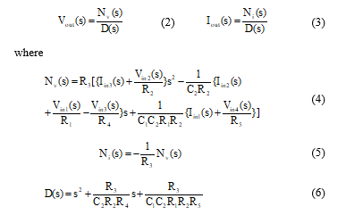
This paper refers to a novel mixed-mode universal biquad employing plus current output differential voltage current conveyors with grounded passive components. The circuit performs mixed-mode operation with the selection of the input and output terminals, and it enables low-pass, band-pass, high-pass, band-stop and all-pass responses choosing suitable input signals. The circuit needs no component matching constraints for obtaining five basic circuit responses above, and can adjust orthogonally the characteristic parameters by the circuit component. Additionally, the circuit has extremely low sensitivities with respect to the circuit components. A circuit design is performed with PSPICE simulation in order to verify the workability of the circuit.
1. Introduction
Active circuit with high performances (i.e. high frequency operation, low power dissipation, wide dynamic range, etc.) is receiving significant attention. Numerous circuit designs using some active devices such as operational trans-conductance amplifiers (OTAs), second generation current conveyors (CCIIs) and differential voltage current conveyors (DVCCs), etc. have been reported in the literature earlier [1-12].
A DVCC is a very useful active device, and DVCC-based circuit is adaptable to wideband operation. A plus current output DVCC (PO-DVCC) is composed of simpler circuit configuration than a minus current output one. Hence it has low power performance compared to the minus current output DVCC. Several voltage-mode (VM) and current-mode (CM) circuits have been synthesized by employing the DVCCs previously [8-11].
A biquad circuit is a typical second-order building block, and it is used for configuring various types of high-order circuits. It is required for circuit designers that the circuit enables some kinds of circuit responses without any component matching constraints, and that it has orthogonal or independent adjusting for characteristic parameters. Additionally, the circuit configuration employed grounded passive components is much recommended for CMOS implementation.
In actuality, active circuit may be claimed to operate in the mixed-modes (i.e. the VM, CM, trans-admittance-mode (TAM) and trans-impedance-mode (TIM)) from a broad viewpoint. So far, there are some research reports concerning OTA-based mixed-mode biquads [1-3]. But the OTA-based biquads above are not applicable to wideband behavior compared with the DVCC-based ones. If the mixed-mode biquad utilizing the PO-DVCCs is devised, the circuit has some excellent performances (i.e. wideband operation, low power dissipation, etc.) in comparison with conventional ones. However, such PO-DVCC-based biquad has not been well researched as yet.
This article focuses on a novel mixed-mode universal biquad using only the PO-DVCCs with grounded passive components as mentioned above. The biquad circuit configuration is consisted of an integrator loop structure with loss-less integrators [4]. The circuit performs the VM, CM, TAM and TIM operations with the selection of the input and output terminals, and it enables the low-pass (LP), band-pass (BP), high-pass (HP), band-stop (BS) and all-pass (AP) characteristics by suitably choosing the input signals with no component matching constraints. The characteristic parameters ω0 and Q are set orthogonally by the circuit components. Additionally, the sensitivity analysis leads that the biquad has extremely low sensitivities with respect to circuit components.
A versatile mixed-mode biquad employing current controlled DVCCs (DVCCCs) is inducted. A DVCCC is an active device utilized effectively the parasitic resistance at the x-terminal of the DVCC. The circuit is composed of plus current output DVCCCs (PO-DVCCCs) and grounded capacitors. And the circuit performance can be controlled electronically with the bias currents of the PO-DVCCCs.
A biquad circuit design is carried out with PSPICE simulation, and the simulation responses are favorable sufficient over a wideband of frequencies. The biquad has several excellent performances in terms of the wideband operation, low power dissipation, orthogonal adjusting for the characteristic parameters, etc., and it suits well for CMOS implementation.
2. Plus current output DVCC
The symbol of the PO-DVCC is given in Figure 1, and hereinto it shows dual plus current output DVCC.
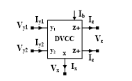 Figure 1: Symbolic representation of PO-DVCC
The PO-DVCC is characterized by the terminal equations [8] below:
![]() The MOS PO-DVCC configuration [11] is shown in Figure 2. It is an active device modified differential difference current conveyor (DDCC) [12], namely one y-terminal with plus polarity is grounded in the DDCC.
The MOS PO-DVCC configuration [11] is shown in Figure 2. It is an active device modified differential difference current conveyor (DDCC) [12], namely one y-terminal with plus polarity is grounded in the DDCC.
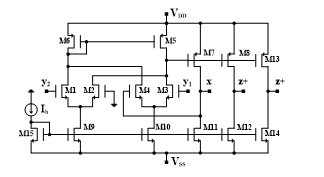 Figure 2: Plus current output DVCC configuration with MOS transistors
3. DVCC-based biquad and its performances
The mixed-mode universal biquad circuit configuration is shown in Figure 3. The circuit is consisted of four single PO-DVCCs, one dual PO-DVCC with grounded resistors and capacitors. This circuit is configured utilizing a second-order loss-less integrator loop structure [4].
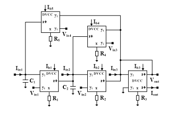 Figure 3: DVCC-based biquad circuit configuration
The voltage and current outputs Vout(s), Iout(s) are given as:
 It is obvious from the equations above that the circuit performs the mixed-mode behavior with the selection of the input and output terminals, and it enables the various kinds of the circuit responses choosing the input signals suitably.
In the CM operation (i.e. Vin1(s)=Vin2(s)=Vin3(s)=Vin4(s)=0), the circuit transfer functions are realized as below:
LP: Iin1(s)=Iin(s), Iin2(s)=Iin3(s)=0
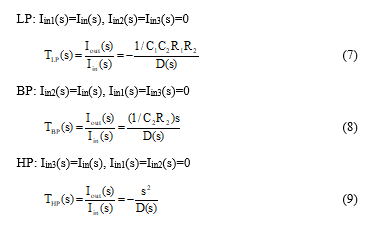
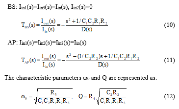 Thus the circuit enables five basic circuit responses with no component matching constraints, and the characteristic parameters ω0 and Q are set orthogonally by the passive components.
Especially the deviation of the circuit components affects the circuit performance. Hence we examine the effects with sensitivity analysis. The component sensitivities concerning ω0 and Q are shown in Table 1. These values clarify that the circuit has low sensitive performance. It is an additional note that the sensitivities are not dependent on the component values.
Table 1: Component sensitivities
| x | ω0 sensitivity | Q sensitivity |
| R1 | -0.5 | -0.5 |
| R2 | -0.5 | 0.5 |
| R3 | 0.5 | -0.5 |
| R4 | 0.0 | 1.0 |
| R5 | -0.5 | -0.5 |
| C1 | -0.5 | -0.5 |
| C2 | -0.5 | 0.5 |
Successively we examine the performance of the VM circuit. The circuit responses in the VM operation (i.e. Iin1(s)=Iin2(s)=Iin3(s)=0) are found with the choice of the input voltages as below:
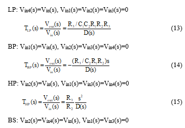
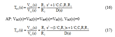 The VM circuit can also realize the LP, BP, HP, BS and AP transfer functions like as the CM one. The characteristic parameters ω0, Q and component sensitivities are same as the current-mode ones.
In addition, the TAM and TIM operations are performed selecting the input terminal Iin(s)/Vin(s) and output terminal Vout(s)/Iout(s), respectively. Also, the circuit responses are derived with the above-mentioned ways in these operational modes.
4. Current controlled DVCC and biquad circuit configuration
In reality, the DVCC has parasitic resistance existing at the x-terminal, and the resistance varies with the bias current. The parasitic resistance Rx is given as:
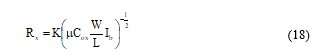 where μ, Cox, W/L, Ib and K denote the electron mobility, gate oxide capacitance per unit area, MOS transistor aspect ratio, bias current and constant parameter, respectively. Equation (18) shows that the parasitic resistance Rx is electronically adjusted with the bias current Ib. An active device made good use of the parasitic resistance is named DVCCC.
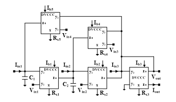 Figure 4: DVCCC-based biquad circuit configuration
Figure 4 illustrates the biquad circuit configuration employing the PO-DVCCCs. The circuit is composed of the PO-DVCCCs and grounded capacitors. The voltage and current outputs Vout(s), Iout(s) are given replacing the external resistance Ri to the parasitic resistance Rxi from (4) to (17). The characteristic parameters ω0 and Q are also obtained with the same replacement.
The PO-DVCCC-based biquad has electronic tunability for the characteristic parameters with the bias currents. In addition, it can be expected that the circuit has a high potential for low power performance, because the circuit configuration is without external resistors.
5. A circuit design and simulation responses
In order to confirm our proposal, we tried to realize a CM circuit using PSPICE simulation. As a circuit design, we deal a specification with the cut-off frequency f0=1MHz, quality factor Q=1.0 and gain constant H=1.0. A macro model of the PO-DVCC in Figure 2 was used in this simulation.
To achieve the specification above, we set that the circuit components were Ri (i=1, 2, 3, 4, 5)=12kΩ and C1=C2=12pF, and that the bias currents (i=1, 2, 3, 4, 5)=10μA, DC supply voltages VDD=-VSS=0.8V and input current Iin=10μA, respectively.
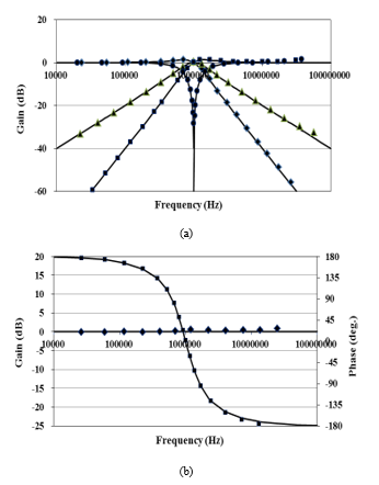 Figure 5: Simulated circuit responses
The simulation responses are given in Figure 5. Figure 5 (a) presents the LP, BP, HP and BS responses, and meanwhile the AP response is indicated in Figure 5 (b). In the figures, the marks signify the simulated responses, and the continuous lines show the theoretical responses. The simulated responses agree very well with the ideal values over a wide range of frequencies. The consumed power dissipation was 0.439mW. It’s rather small.
The MOS transistor aspect ratios [10] are given in Table 2. Additionally, we utilized device parameters of MOSIS 0.5μm for other parameters.
Table 2: MOS transistor aspect ratios.
| MOS transistors | W / L |
| M1-M4 | 20μm / 0.5μm |
| M5-M8, M13-M15 | 30μm / 2μm |
| M9-M12, M16-M19 | 10μm / 2μm |
6. Conclusions
In this paper, we have proposed a novel mixed-mode universal biquad employing plus current output DVCCs with grounded passive components. Additionally, we demonstrated that the circuit accomplishes the mixed-mode behavior, and it enables five kinds of basic circuit responses without any component matching constraints. The circuit is capable of orthogonally adjusting the characteristic parameters by the circuit components. It has also been revealed that the component sensitivities were extremely low in the circuit.
The versatile plus current output DVCCC-based biquad has been inducted. The circuit can adjust electronically the circuit performances with the bias currents.
A circuit design was performed with SPICE simulation, and the simulated responses were sufficient good over a wideband of frequencies.
Our proposed biquad possesses several advantages concerning the wideband operation, low power dissipation, orthogonal adjusting for the characteristic parameters, etc., and it is easily capable of integrating in CMOS technology.
In reality, the DVCC has non-ideal elements (i.e. voltage and current tracking errors, etc.), and especially they affect the circuit performances. An appropriate solution on this must be found out in the future.
Acknowledgment
The authors would like to thank to Mr. David Martin for his helpful suggestions. Especially we are grateful to him for editing our manuscript properly.
- M.T. Abuelma’atti, et al, “A novel mixed-mode OTA-C universal filter” Int. J. Electron., 92(7), 375-383, 2005. https://doi.org/10.1080/08827510412331295009
- C.N. Lee, “Multiple-mode OTA-C universal biquad filters” Cir. Syst. Sig. Proc., 29, 263-274, 2010. DOI 10.1007/s00034-009-9145-0
- T. Tsukutani, et al, “A mixed-mode biquad employing OTAs and grounded capacitors” J. Elec. Eng., 6(3), 151-155, 2018. DOI: 10.17265/2328-2223/2018.03.003
- E. Sanchez-Sinencio, et al, “Generation of continuous-time two integrator loop OTA filter structures” IEEE Trans. Cir. Syst., 35(8), 936-946, 1988. DOI: 10.1109/31.1840
- Y. Tao, J.K. Fidler, “Electronically tunable dual-OTA second-order sinusoidal oscillators/filters with non-interacting controls: a systematic synthesis approach” ibid., 47(2), 117-129, 2000. DOI: 10.1109/81.828566
- S.H. Tu, et al, “Novel versatile insensitive universal current-mode biquad employing two second-generation current-conveyors” Int. J. Electron., 89(12), 897-903, 2002. https://doi.org/10.1080/0020721031000121262
- J.W. Horng, “High input impedance voltage-mode universal biquadratic filters with three in-puts using plus-type CCIIs” ibid., 91(8), 465-475, 2004. https://doi.org/10.1080/00207210412331294612
- H.O. Elwan, A.M. Soliman, “Novel CMOS differential voltage current conveyor and its applications” IEE Proc. Cir. Dev. Syst., 144(3), 195-200, 1997. DOI: 10.1049/ip-cds:19971081
- M.A. Ibrahim, et al, “A 22.5MHz current-mode KHN-biquad using differential voltage current conveyor and grounded passive elements” Int. J. Electron. Com., 59, 311-318, 2005. https://doi.org/10.1016/j.aeue.2004.11.027
- S. Minaei, M.A. Ibrahim, “General configuration for realizing current-mode first-order all-pass filter using DVCC” Int. J. Electron., 92(6), 347-356, 2005. https://doi.org/10.1080/00207210412331334798
- T. Tsukutani, et al, “Novel current-mode bi-quadratic circuit using only plus type DO-DVCCs and grounded passive components” ibid., 94(12), 1137-1146, 2007. DOI: 10.1080/00207210701791085
- W. Chiu, et al, “CMOS differential difference current conveyors and their applications” IEE Proc. Cir. Dev. Syst., 143(2), 91-96, 1996. DOI: 10.1049/ip-cds:19960223
No related articles were found.