A Dual-Band 90-Degree SiGe HBT Active Phase Shifter Based on Band-Pass and Band-Stop Designs Using Dual-Band Resonators

Adv. Sci. Technol. Eng. Syst. J. 3(4), 224–229 (2018);
 DOI: 10.25046/aj030421
A dual-band 90-degree SiGe HBT active phase shifter based on band-pass and band-stop designs using dual-band resonators is presented in this paper. The active phase shifter employs differential configuration and has band-pass and band-stop filters in the load circuit. By switching two output ports of the differential amplifier, 90-degree phase shifting has been realized at dual bands. The implemented dual-band active phase shifter using 0.35 micron SiGe HBT has achieved a gain of 9.3 dB and a phase shift of 95 degrees at 0.74 GHz as well as a gain of 8.9 dB and a phase shift of 98 degrees at 0.88 GHz. This is the first paper to present a dual-band active phase shifter based on band-pass and band-stop designs using dual-band resonators.
1. Introduction
This paper is an extension of the work originally presented in the 47th European Microwave Conference, 2017 [1]. Recently, multi-band phase shifters are being developed for the next generation multi-band and multi-mode wireless communication systems using active phased array modules and/or beam-forming networks [2]-[3]. Various types of multi-band phase shifters have been reported, including reflection-type [4]-[5], loaded-line type [6]-[7], vector-sum type [8] and wideband distributed amplifiers with varactor-tuned LC networks [9]-[10]. However, there was no report on the low-pass high-pass phase shifters for the multi-band or multi-mode applications. In order to address this issue, a novel dual-band active phase shifter using band-pass and band-stop designs has been presented in [1]. The active phase shifter is based on a differential amplifier and employs two types of different loads, that is, band-pass or band-stop filters. With the use of abrupt phase shifting characteristics at around cutoff frequencies of the filters [11]-[12], variable phase shifting can be easily achieved at multiple bands by switching band-pass and band-stop filters. Although the conventional low-pass high-pass phase shifters [13]-[14] are limited to single-band operation, band-pass and band-stop designs can make multi-band operation available. In [1], 90-degree phase shifting has been successfully achieved at dual-band by switching two output ports of the differential amplifier. From the viewpoint of multi-band phase shifting as well as high gain, the active phase shifter is considered to be one candidate for achieving various phase shifting at multiple bands, which would be used in the next generation multi-band or multi-mode wireless communication systems with active phased array antenna and beam forming networks. To extend the work [1], the dual-band passive phase shifter based on band-pass and band-stop designs is newly described, showing that the dual-band 90-degree phase shifting is unavailable because of a low Q-factor of the circuit elements. Then how to address this design issue is presented by utilizing 180-degree out of phase performance of the differential amplifier. It is also added in description that an impedance matching has to be taken into account since the band-pass and band-stop filters using dual-band resonators are actually employed in the output matching circuit of the differential amplifier. The outstanding features of the multi-band active phase shifter based on band-pass and band-stop designs over the previously published multi-band phase shifters are high gain and digital control. Thus the measured input and output return losses are newly added for multi-bit applications.
In Chapter 2, the design, simulation, fabrication and performance of the dual-band band-pass/band-stop switching passive phase shifter are presented, showing that the dual-band 90-degree phase shifting becomes unavailable because of a low Q-factor of the circuit elements. In Chapter 3, the design, simulation, fabrication and performance of the dual-band band-pass/band-stop switching active phase shifter are presented, showing that the dual-band 90-degree phase shifting becomes available by utilizing 180-degree out of phase performance of the differential amplifier. Moreover, it is clearly shown as a comparative analysis that the dual-band active phase shifter based on band-pass and band-stop designs has an advanced feature in performance and controllability over the previously published multi-band phase shifters.
2. Dual-Band Band-Pass/Band-Stop Switching Passive Phase Shifter
2.1. Circuit Design
A schematic diagram of the dual-band band-pass/band-stop switching passive phase shifter is shown in Figure 1. It employs band-pass/band-stop filters comprised of dual-band resonators and SPDT switches. A 90-degree phase shifting can be accomplished by switching band-pass and band-stop filters.
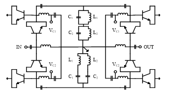 Figure 1: Schematic diagram of the dual-band band-pass/band-stop switching passive phase shifter
A dual-band phase shifting technique by switching band-pass and band-stop filters is illustrated in Figure 2. Figures 2(a) and 2(b) present band-stop and band-pass filters, respectively. The magnitude and phase shift of the band-stop and band-pass filters are illustrated in Figure 2(c) and Figure 2(d), respectively. The band-stop filter is comprised of two parallel LC circuits in a stacked form. It has a single band-stop frequency of f3a and dual band-pass frequencies of f1 and f2, which are given as the following equations [11]-[12]:
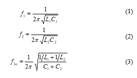 On the other hand, the band-pass filter is constructed from two series LC circuits. It has a single band-pass frequency of f3b and dual band-stop frequencies of f1 and f2. f3b is given as the following equation [11]-[12]:
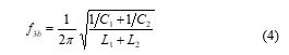
 Figure 2: Dual-band phase shifting technique by switching band-pass and band-stop filters
At around transition frequencies in Figure 2(c), the impedance drastically changes from open to short, or short to open. Moreover, a low-pass filter shows a negative phase shift and a high-pass filter provides a positive phase shift. Due to the actual low Q factor, however, the phase shift obtained by switching band-pass/band-stop filters has a limit shown in Figure 2 (d). Now it is assumed that the gain is expressed as Ga, Gb and the phase shift is DFa, DFb at the frequency points a or b, respectively. The circuit design has to focus mainly on how to determine L1, C1, L2 and C2 to meet with Ga = Gb and/or DFa = DFb at dual-band of the frequency points a and b.
2.2. Circuit Simulation
A circuit simulation is performed by using ADS2016 for the schematic diagram shown in Figure 1. 1005-type chip elements are used as R, L or C as well as 0.35 mm SiGe HBT with an ft of around 25GHz is used as a switching element by taking into account the operating frequency around L-Band as well as better performance of SiGe HBTs over CMOS devices. The circuit element values are listed in Table 1. The simulated S21 and a phase shift DF is shown in Figure 3. At the frequency points a and b, DF becomes around 80 and 50 degrees, respectively
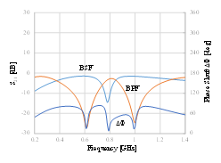 Figure 3: Simulated S21 and a phase shift DF
2.3. Circuit Fabrication and Performance
A photograph of the dual-band band-pass/band-stop switching passive phase shifter is shown in Figure 4. The phase shifter was fabricated on the FR-4 substrate with a dielectric constant of 4.4 @ 1 GHz and a tand of 0.016 @ 1 GHz. 1005-type chip resistors, capacitors, and inductors are mounted on the substrate by soldering. A surface mount type of the 0.35 mm SiGe HBT with an ft of around 25 GHz (Toshiba MT4S102T) is used as a switching device. The circuit size is 16 x 16 x 1.2 mm3.
The measured S21 and phase shift of the dual-band band-pass/band-stop passive phase shifter are demonstrated in Figure 5. The measured results are basically in good agreement with the simulated results of Figure 3. A slight discrepancy appears for the phase shifting value at Ga and Gb. This is most likely due to the error in the modeling of Q-factor. Bias conditions are VC1=-1V and VC2=+1V for BPF as well as VC1=+1V and VC2=-1V for BSF.
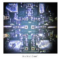 Figure 4: Photograph of the dual-band band-pass/band-stop switching passive phase shifter
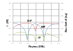 Figure 5: Measured S21 and phase shift of the dual-band band-pass/band-stop switching passive phase shifter
3. Dual-band Active Phase Shifter Based on Band-Pass and Band-Stop Designs Using Dual-Band Resonators
3.1. Circuit Design
A schematic diagram of the dual-band active phase shifter based on band-pass and band-stop designs is shown in Figure 6. It is comprised of a differential amplifier and a SPDT switch. The differential amplifier employs two different loads of ZL1 and ZL2. ZL1 corresponds to the band-stop filter in Figure 2(a) and ZL2 in Figure 2(b). To supply a voltage to differential transistor pairs, a large inductance of L3 (100nH) is connected in parallel with C1 and C2. ZS is a series feedback circuit comprised of two resistors RS. RE is a current source. Differential outputs of OUT+ and OUT- are connected to a SPDT switch.
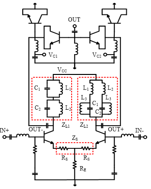 Figure 6: Schematic diagram of the differential amplifier and dual-resonant RLC circuit
The SPDT switch employs a series-shunt configuration for a high isolation. Since the collector and emitter are short-circuited, the transistor acts as a switching diode. VC1 and VC2 are a control voltage. Input matching circuits employ a lossy match configuration to improve an input matching as well as stabilize the circuit. The base bias resistors for a differential transistor pair are not shown in Figure 6 because of a circuit simplicity. VCC is a supply voltage.
The phase shifting performances are compared for the passive phase shifter of Figure 1 and the active phase shifter of Figure 6, which is shown in Figure 7. Since the output signal from the differential amplifier is already 180 degrees out of phase, the phase shifting performance of the active phase shifter is a complementary value of the passive phase shifter.
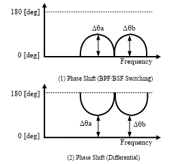 Figure 7 Phase shifting performances of the passive phase shifter (Figure 1 and the active phase shifter (Figure 6)
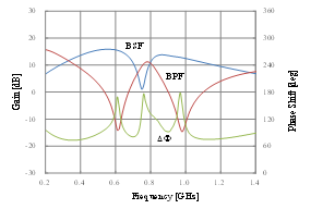 Figure 8: Simulated gain and phase shift of the dual-band active phase shifter using band-pass and band-stop designs
3.2. Circuit Simulation
The circuit simulation has been done by using ADS2016 for the schematic diagram in Figure 6 with the circuit element value of Table 1. VCC is 6 V. VC1 and VC2 are +1 V or -1 V. Simulated gain and phase shift of the dual-band active phase shifter using band-pass and band-stop designs are shown in Figure 8. First, it is clearly shown that 180-degree phase shifting has been obtained at f1, f2, f3a or f3a. Moreover, a phase shift of 80 to 180 degrees can be realized between f1 and f3a or f3b as well as between f2 and f3a or f3b. It must be noted that the phase shifting value is greatly dependent on the frequency separation of f1 and f2 in addition to Q-factors of the band-pass and band-stop filters.
3.3. Circuit Fabrication and Performance
A photograph of the dual-band active phase shifter using band-pass and band-stop designs is shown in Figure 9. In a similar way as Figure 4, the active phase shifter was fabricated on the FR-4 substrate with a dielectric constant of 4.4 @ 1 GHz and a tand of 0.016 @ 1 GHz. 1005-type chip resistors, capacitors, and inductors are mounted on the substrate by soldering. A surface mount type of the 0.35 mm SiGe HBT with an ft of around 25 GHz (Toshiba MT4S102T) is used as an amplifier device as well as a switching device. The circuit size is 16 x 16 x 1.2 mm3. The circuit has two SMA connectors on the bottom side for differential inputs and a single SMA connector on the upper side for the output of the SPDT switch.
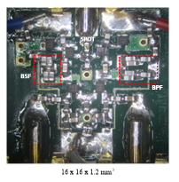 Figure 9: Photograph of the dual-band active phase shifter using band-pass and band-stop designs
The measured gain and phase shift of the dual-band active phase shifter using band-pass and band-stop designs using dual-band resonators are demonstrated in Figure 10. The measured results are basically in good agreement with the simulated results of Figure 8. The active phase shifter has achieved a gain of 9.3 dB and a phase shift of 95 degrees at 0.74 GHz as well as a gain of 8.9 dB and a phase shift of 98 degrees at 0.88 GHz. Small gain ripples appear in Figure 10. This is most likely due to the stability problem. Although the stability problem can be improved with the use of the load resisters, the phase shifting amount becomes smaller due to a low Q-factor, which provides a design tradeoff. Bias conditions are VCC=6 V and VC1, VC2=+1V or -1V, respectively.
The measured input and output return losses of the dual-band active phase shifter using band-pass and band-stop designs are demonstrated in Figures 11 and 12, respectively. The input return loss was 11.8 dB at 0.74 GHz and 16.3 dB at 0.88 GHz. The output return loss was better than 8 dB at both 0.74 GHz at 0.88 GHz. As mentioned above, the load resistor also improves the output return loss but the Q-factor becomes worse.
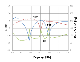 Figure 10: Measured gain and phase shift of the dual-band active phase shifter using band-pass and band-stop designs
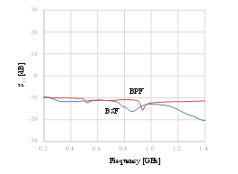 Figure 11: Measured input return loss of the dual-band active phase shifter using band-pass and band-stop designs
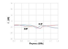 Figure 12: Measured output return loss of the dual-band active phase shifter using band-pass and band-stop designs
3.4. Comparative Analysis
A comparative analysis is summarized in Table 2. Since this paper is the first report on the dual-band phase shifter using BPF/BSF or LPF/HPF switching, the results obtained from this work are compared with the other multi-band phase shifting methods. All of the multi-band phase shifters in Table 2 have achieved a multi-band phase shifting by switching devices or circuits. The reflection type [4] and the loaded-line type [6] are based on passive phase shifter designs and thus the insertion loss is large. On the other hand, the vector-sum type [8] and our work [1] are an active phase shifter and thus have an insertion gain. Moreover, the phase shifters in [4], [6] and [8] are analogously controlled and thus the complex control is needed. It can be concluded from these viewpoints that the dual-band phase shifter using band-pass and band-stop designs of our work can provide several advantages especially in performances and controllability over the previous ones.
4. Conclusions
Design, fabrication and performance of the dual-band active phase shifter based on band-pass and band-stop designs using dual-band resonators have been presented. It can be clearly shown that the dual-band 90-degree phase shifting is unavailable for the passive phase shifter merely using band-pass and bandstop switching but becomes available for the active phase shifter using a differential amplification. The implemented dual-band active phase shifter using 0.35 mm SiGe HBT has achieved a gain of 9.3 dB and a phase shift of 95 degrees at 0.74 GHz as well as a gain of 8.9 dB and a phase shift of 98 degrees at 0.88 GHz. 180-degree phase shift can be easily obtained with the use of the differential amplifier, In addition, a lower bit of 45-, 22.5- and 11.25-degrees can be achieved by using the same band-pass and band-stop designs. With the use of these techniques, digitally-controlled 5-bit multi-band active phase shifters having a high gain can be realized for use in the next generation, multi-band and multi-mode wireless communication systems.
- Y. Itoh, H. Takagi, “A Dual-Band 90-Degree SiGe HBT Active Phase Shifter Using Band-Pass and Band-Stop Designs”, in 47th European Microwave Conference, pp. 232-235, October 2017.
- T. Nakagawa, M. Kawashima, H. Hayashi, K. Araki, “A 0.9-2.5 GHz Wideband Direct Conversion Receiver”, in IEEE GaAs IC Digest, pp. 37-40, 2001.
- H. Kamizuma, T. Yamawaki, Y. Akamine, K. Maeda, S. Tanaka, “A Quad Band WCDMA Transceiver with Fractional local divider”, in Symposium on VLSI Circuits Digest, pp. 96-99, 2008.
- Ocera, E. Sbarra, R. Vincenti Gatti, R. Sorrentino, “An Innovative Reconfigurable Reflection-Type Phase Shifter for Dual Band WLAN Applications”, in European Microwave Association, pp. 64-67, 2006.
- Y. Shoji, K. Sakamoto, Y. Itoh, “A Dual-Band Reflection Type Phase Shifter Using Active Loads”, in Contemporary Engineering Sciences, Vol. 7, No. 20, pp. 957-964, 2014.
- N. Park, J. Gwan, Y. Kim, C. Lee, “Dual-band Switching Doherty Power Amplifier using Phase Shifter Composed of PIN Diode”, in 6th European Microwave Integrated Conference, pp. 300-3003, 2011.
- M. Maassel, B. D. Braaten, D. A. Rogers, “A Metamaterial-Based Multiband Phase Shifter”, in IEEE International Conference on Electro/Information Technology, pp. 533-535, 2014.
- D. R. Banbury1, N. Fayyaz2, S. Safavi-Naeini1, S. Nikneshan, “A CMOS 5.5/2.4 GHz Dual-band Smart-antenna Transceiver with a Novel RF Dual-band Phase Shifter for WLAN 802.11a/b/g”, in IEEE RFIC Symposium Digest, pp. 157-160, 2004.
- Lu, A. Pham, D. Livezey, “On the Linearity of CMOS Multi-band Phase Shifters”, in Topical Meeting on Silicon Monolithic Integrated Circuits in RF Systems, Page 4, pp., DOI: 10.1109 /SMIC.2005.1587973, 2006.
- Z. El-Khatib, L. MacEachern, S. A. Mahmoud, “Fully-Integrated Multi-band Tunable Linearized CMOS Active Analog Phase Shifter with Active Loss Compensation for Multiple Antenna Wireless Transceiver Applications”, in International Symposium on Circuits and Systems, pp. 2966-2969, 2009.
- G. L. Matthaei, L. Young, E.M.T. Jones, Microwave Filters, Impedance-Matching Networks, and Coupling Structures, Artech House, ISBN: 978-0-89006-099-5, 1965.
- M. Poger, “Microwave engineering education: From field theory to circuit theory”, in IEEE/MTT-S International Microwave Symposium Digest, 2012.
- Y. Ayasli, S. W. Miller, R. Mozzi, L. K. Hanes, “Wide-Band Monolithic Phase Shifter”, in IEEE Trans. ED-31, No. 12, pp. 1943-1947, 1984.
- J. P. Comeau, M. A. Morton, J. D. Cressler, J. Papapolymerou, M. Mitchell, “A High-Linearity 5-bit, X-band SiGe HBT Phase Shifter”, in IEEE MTT-S Digest, pp. 1668-1671, 2006.