Three port converters used as interface in photovoltaic energy systems
Three port converters used as interface in photovoltaic energy systems
Volume 3, Issue 2, Page No 263-270, 2018
Author’s Name: Sarab Al-Chlaihawi1,2,a), Aurelian Craciunescu2
View Affiliations
1Al-Furat Al-Awsat Technical University, Center Education Continuous, 54001, Iraq
2Electrical Engineering Faculty, University Politehnica of Bucharest, 060042, Romania
a)Author to whom correspondence should be addressed. E-mail: sarab.haedar@yahoo.com
Adv. Sci. Technol. Eng. Syst. J. 3(2), 263-270 (2018); ![]() DOI: 10.25046/aj030231
DOI: 10.25046/aj030231
Keywords: Three port converter, DC-DC converter, PV panel, MPPT, Full bridge converter

Export Citations
The aim of this paper is to derive and study a full-bridge three-port converter. Based on the standard design of full-bridge converter, we have modeled and derived a three port converter. The three port converter can be used in renewable energy scenarios, such as solar cells or wind turbines connected to the input port. The input can be taken from two-ports simultaneously or from one port at a time. In order to balance the power mismatch between the input port and load port, the batteries are attached to the third port, to ensure there are no discrepancies in the power generated at the input and power demand at the load. In order to ensure isolation and reduced voltage stress on the switches, a high frequency transformer is also used in the design. The overall design contains four switches, and four diodes. MOSFETs are the strongest candidate for the switches owing to their high switching speed, lower losses and high resistance to higher voltage. Moreover, a buck-boost structure is modeled in order to ensure that it can work for a wide variety of different applications by adjusting the duty cycle of the switches properly. To minimize the switching losses in the converter, Zero-Voltage Switching (ZVS) is also achievable in the modeled system.
Received: 12 January 2018, Accepted: 03 April 2018, Published Online: 25 April 2018
1. Introduction
Multiport converters have the inherited advantage of being compact and handy, unlike the traditional converters. Instead of using multiple two-port converters for various applications involving power flow between different ports, three-port converters which feature single-stage conversion between different ports are more desirable; they provide higher efficiency, fewer components, compact-design and reduced switching losses. This is possible because switching and storage elements are shared between different ports and hence less component count yields better efficiency. Moreover, the unified power flow management is possible in multiport converters due to centralized control which boosts dynamic performance of the system. The centralized control enables the system to operate without any possibility of communication delay or errors, since it doesn’t require any communication between control units of different converters. This paper is an extension of work originally presented in conference the 10th international symposium on advanced topics in electrical engineering [1]. Where we have analyzed the state equations, inductor volt-second balance for each state, analyzed the design parameters of the system and how different parameters depend on inductor currents, transformer turn ratio and output load current, analyzed the effect of different duty ratios on the battery and output current and we have analyzed the Zero-Voltage Switching mechanism in the modeled converter. Recently, many researches have been carried out on the topology of the multiport converters; for example, one research proposed to interface multiple converters to a common dc bus, each one having its own control unit [2]. But, it has been established that integrated topology carries definite advantages over multiple converters. Owing to these capabilities, three-port converters have gained popularity in recent years. Three-port converters can be constructed using different topologies such as series-resonant, full-bridge and half-bridge with the use of multi-winding transformers [3]. The power flow management and Zero Voltage Switching (ZVS) can be achieved in three-port converters using phase-shift control between different switching bridges [4]. However, an N-port converter contains N-1 control inputs; that is two control inputs for a three-port converter. As a consequence, modeling effort is increased, which results in complicated control circuit, which can offset the good efficiency of the system, if not properly designed. It also requires proper decoupling of different control loops since it contains integrated power stage [5].
The multiport topologies can be isolated or non-isolated, depending upon the application for which they are being used [6].
Isolated converters are preferred in applications when a huge step is desired between input and output voltages. Isolated converters based on bridge topology renders good efficiency in such cases, when combined with soft switching methods [5]. Full-bridge configuration is used where converter power levels are beyond 750 W. It is not recommended for applications below this power level since it has a higher number of electronic components present—it has four transistor switches and associated controller circuit [7].
As the transformer’s magnetizing current is bipolar, the full-bridge’s utilization of transformer core is very efficient, since the entire cycle of B-H loop is used by the full-bridge. Usually the secondary winding is center-tapped and each half of the secondary winding forward the input power during alternate switching periods. This results in winding power loss due to secondary winding current. A schematic of general full-bridge converter with one secondary winding is shown in Figure 1. It contains four switches SA1, SA2, SB1, SB2, transformer with inductance Lm, four diodes and an inductor Lf to filter out the ac components in the output voltage level.
2. Derivation of Three Port Converter
In order to derive the design of three port converter, again consider the Figure 1. It has two legs of switches, which are connected to the source Vs in parallel. The volt-second balance of the transformer inductance Lm represents the constraint condition of the full bridge converter. This implies that if inductance Lm satisfies the volt-second balance, then both the legs of the converter can be divided into two separate portions, known as cell A and cell B. This is shown in Figure 2.
Furthermore, to introduce the battery in the system, we can connect cell A and cell B to different sources, such that cell A is connected to a source Vsa and cell B is connected to the battery source Vsb. If Vsa is equal to Vsb, the original full-bridge converter is derived. Hence, three port full-bridge converter is a general case in which Vsa and Vsb are assumed to be different sources with different voltage. When both the voltages are always equal, the cells are paralleled again. The converter assumes the shape as shown in Figure 3. It is obvious that the proposed three port full-bridge converter has a symmetric configuration in which both the sources can equally participate in supplying the power to the load. The primary winding inductance Lm can act as an inductor, which implies that primary side of the converter contains an inherent buck-boost converter with bidirectional characteristics.
This feature makes this design even more flexible in terms of power transfer between the two sources i.e. the power flow can be managed between the two sources as required, such as PV sources charging the batteries. Either of the voltage sources can be at higher or lower potential than the other.
The concept of primary side buck-boost converter is illustrated in Figure 4. The proposed converter with three ports is suitable for systems which combine renewable energy sources and energy storing devices, since the power flow is possible between the sources. The sources can be PV arrays, wind turbines etc.
The most suitable and commonly used energy storing devices are Lithium-Ion battery or hybrid battery and super-capacitors. Any input power can be transferred to output load in a single-stage, without introducing any additional devices or components in the original full-bridge converter. In order to eliminate switch losses, the converter can be operated with Zero-Voltage Switching for all switches by using primary inductance Lm as energy storage component [8].
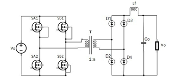 Figure 1-Full Bridge Converter
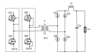 Figure 2- Splitting of Full Bridge Converter
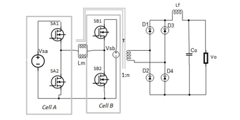 Figure 3-Three port full bridge converter
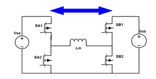 Figure 4-Primary Side of Buck-Boost
3. Full Bridge Three Port Converter
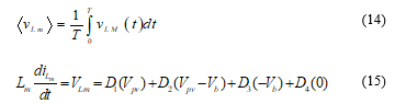
The three-port full-bridge converter with Photo Voltaic (PV) panel and battery bank is shown in Figure 5. As proposed, it has four switches which can transfer the power between PV array, the controller for Maximum Power Point Tracking (MPPT), batteries and one transformer with turn ratio 1:n, which steps up the voltage to drive the load. The Maximum Power Point Tracking is a mandatory circuit which is used with PV array to ensure that at the given sunlight intensity, maximum power is harnessed from the PV cells. Switches SA1 and SA2 provide an interface for the PV panel with a unidirectional flow from the PV panel, while switches SB1 and SB2 are connected to the battery port and provide bidirectional flow from and to the battery. This configuration is necessary since PV panels cannot intake power while batteries have to both charge and discharge over the course of the operation.
The positive of the battery bank is connected with the switch SB1 and negative connected at the SB2. The battery serves as an input when the SB1 is turned on. Both the PV array and batteries can arrange power for the load in a Dual Input Single Output fashion. In fact, the converter can operate in 3 modes, which are explained later. In order to smoothen the output voltage, a rectifier circuit is also connected at the load side, which consists of four diodes and a capacitor C1. The circuit parameters are summarized in Table 1.
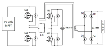 Figure 5- Three-port converter with PV panel and battery bank
A transformer is required to isolate the load output from the PV array and batteries. The transformer is also required to reduce the stress on the switches when the difference between input and output voltages is higher.
This helps in reducing the switch losses in the system. Since the transformer is introduced inside the buck-boost configuration of the converter, it has a higher frequency which depends on the switching frequency of the switches. This enables us to use much smaller transformers, even though the converter provides an output voltage within the frequency range of 50-60 Hz.
Table 1- Parameters of the full bridge three port converter
| Component | Value |
| Transformer Frequency | 10kHz |
| Transformer ratio | 1:1 |
| Output Capacitor (C1) | 0.01F |
| Capacitor(Buck-boost ) | 4700μF |
| Inductor (Buck-boost) | 47mH |
| Capacitor (PV panel) | 100μF |
| Magnetizing Inductance (Lm) | 50 H |
| Battery | 12 V |
| Load | 100 W |
| PV Irradiance | 500 W/m2 |
| PV Maximum Power | 150 W |
3.1. Switching Modes of Three-Port Converter
In the ideal conditions, the power flow in the converter can be explained by the equation:
In this equation, Ppv represents power from the PV panel, Pb is battery power and Po is the output power. There are three possible modes in the converter:
- Single Input Single Output
- Single Input Dual Output
- Dual Input Single Output
The converter operates in Mode 1 when Pb= 0, that is, PV panel generates all power and meets the demand at the load side. In Mode 2, Ppv>Po; the PV panels generate redundant power which goes into charging the batteries along with driving the load. In Mode 3, Ppv< Po and PV array and batteries together supply the power to the load.
These modes have been made possible due to the flexible buck-boost structure of the converter. A summary of these modes is depicted in Table 2, while the functionality of each mode is explained in detail in the following section.
Table 2- Modes of the three port converter
| Mode | PV Power Level | Battery Power Level |
| Single Input Single Output | Ppv= Po | Pb=0 |
| Single Input Dual Output | Ppv>Po | Pb>0 |
| Dual Input Single Output | Ppv< Po | Pb<0 |
Mode 1
In mode 1, the configuration of the circuit is shown in Figure 6. Being a single input single output configuration, only PV panel feeds the power to the load. At the end of each cycle, the battery is also charged as evident from Figure 15, when SB1 turns ON and SB2 turns OFF. During the operation in Mode 1, the PV panel generates power to drive the load. However, the battery also gets charged slightly at the end of each switching period. The main flow of power is from PV panel to the output load via switches SA1 and SB2.
The voltage at the primary side of transformer is then boosted by a factor of ‘n’, which represents turns ratio at the secondary side. At the secondary side, diodes D1 and D4 are forward biased as the polarity of secondary voltage is positive at the top side.
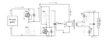 Figure 6- Mode 1 of the modeled converter
Mode 2
Mode 2 is the single input dual output mode, hence PV panels have enough power to feed the load side as well as charging the battery via the switch SB1 whose duty cycle is increased to the maximum value. The configuration for mode 2 is shown in Figure 7.
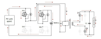 Figure 7- Mode 2 of the modeled converter
In Mode 2, PV panel alone feeds the load and charges the batteries. The PV panel charges the batteries through switch SB1 while catering to the demand of the load via switch SA1. The inherent buck-boost characteristics boost the PV voltage at the primary side of the transformer to a higher value. At the secondary side, diodes D1 and D4 are turned on and supply the positive voltage to the load.
Mode 3
Mode 3 represents the Dual input single output scenario, where the PV panel’s generated power is not sufficient to drive the load; hence the batteries join in to cater to the needs of the load. However, when PV=0, for example during night, the battery has to provide the power to the load all alone, this is shown in Figure 8. Hence, the capacity of the batteries should be decided by considering the expected load. In mode 3, power flow is from batteries to the load via switch SB1 and the transformer.
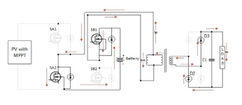 Figure 8-Mode 3 of the modeled converter
3.2. Switching States
In this section, we analyze the different switching states within the converter operations. Irrespective of the mode of the converter, the switching states are same. The only difference the modes make is in the value of inductor current iLm, which changes with the power generated at the PV panel Ppv and power at the load Po. This current change in different modes in terms of value and direction. Below is the case study for the Dual Output mode of the converter. It is assumed that output capacitor C1 is large enough, three voltages Vpv, Vb and Vo are stable during the operation, once the steady state of the converter is reached and that Vpv> Vb.
State I [t0-t1]: At the time t0, switches SA1 and SB2 are ON, while SA2 and SB1 are OFF. The equations for inductor voltage VLm and capacitor current ic1 are as under.
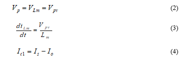 Where Vp is the voltage at the primary side of the transformer while Is is the current at the secondary turn.
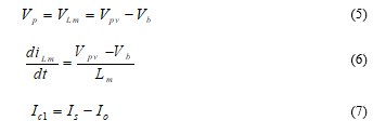
State II [t1-t2]: During this time interval, switches SA1 and SB1 are ON, while SA2 and SB2 are OFF. The equations for inductor voltage VLm and capacitor current ic1 are as under.
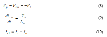
 State III [t2-t3]: During this time interval, switches SA2 and SB1 are ON, while SA1 and SB2 are OFF. During state III, battery supplies power to the load alone. If the power generated at the PV panels becomes is not utilized during this state and is isolated from the rest of the system.
In Figure 8, it is shown that the flow of power is from the battery to the load side via the switch SB1. On the secondary side, diodes D2 and D3 are turned on, due to negative voltage appearing at the secondary top side. The equations for inductor voltage VLm and capacitor current ic1 are as under.
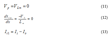
 State IV [t3-t0]: During this time interval, switches SA2 and SB2 are ON, while SA1 and SB1 are OFF. This configuration isolates the PV source and battery from each other and the output. Hence, during interval, inductor current iLm freewheels through the switches SA2 and SB2, while output voltage is maintained by the output capacitor C1.
The equations for inductor voltage VLm and capacitor current ic1 are as under.
 3.3. Volt-Second Balance
If we assume that small ripple approximation, writing the volt-second balance for the primary inductance Lm, the following equation can be obtained.
 3.4. ZVS Analysis
The operation of the proposed Full-Bridge Three Port Converter is almost similar to the operation of a conventional full-bridge converter, except for the difference that in our converter, the primary inductance of transformer is also used as an inductor. Zero Voltage Switching can be realized in this converter using inductors, leakage inductances and drain-to-source capacitances (CDS) of the switches, only if the currents iLm and ip have the similar signs. This is explained in Figure 9, where we have explained SA2 as an example for the Zero-Voltage Switching.
If the leakage inductance of the transformer is LK (as shown in Figure 9), then during state III, when SB1 is ON and SA1 OFF, the primary transformer current becomes ip= iLm+nIs and leakage inductance LK and transformer inductance Lm would release energy that would charge the CDS capacitances of SA1 and SA2.
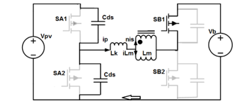 Figure 9-Zero-Voltage Switching in SA2
4. Controller Design
The controller for the converter is designed in Simulink which generates PWM signal for the four switches used in this converter. It is shown in Figure 10. It consists of a MATLAB function block with two inputs, which decide the mode of operation of the converter.
The input 1 initiates mode 1, while input 2 has two parameters, named PV power and Load demand, on the basis of which, mode 2 and 3 are decided. If power at PV is higher than load demand, mode 2 is activated and if load demand is higher than the PV power, mode 3 is activated. On the other side, there are 3 outputs of the MATLAB based controller.
The output SA represents the control signal for switches SA1 and SA2, SB represents the output for switches SB1 and SB2, while the third output C is a control output that controls the delay in the pulses SA and SB. It is to be noted that each pair of switches i.e. SA1/SA2 and SB1/SB2 operate in the complementary fashion, hence one input signal is enough for each pair of switches.
 Figure 10- Design of controller for PWM Generation
5. Modeling of PV panel and controller
Photo Voltaic cells provide the cheapest and cleanest energy; however, their efficiency is lower than other modes. In order to utilize the maximum output of the PV arrays, different control mechanism are suggested which are given the name Maximum Power Point Trackers (MPPT). The solution involves the use of I-V characteristic curve of the solar panels and making the PV system operate at the point on the curve that gives maximum power known as Maximum Power Point. In the given I-V curve, as shown in Figure 11, the current value depends on the sunlight evident at the cells. The current can be calculated using the following equation:
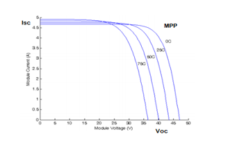 Figure 11-Typical I-V curve with dependence on incident sunlight
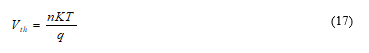
The Vth refers to the thermal voltage given by following equation:
 As shown in Figure 11, when the voltage of the I-V curve approaches zero, at that time the current from the PV panel is maximum, which is called Short Circuit current (Isc). It depends on the properties of the cells such as absorption and reflection constant and incident light etc. Similarly on the opposite extreme, the point at which the current approaches zero, that voltage as known as Open Circuit Voltage (Voc), which is the maximum attainable voltage by the PV panel. It depends on the material used in the solar panel, e.g. silicon solar cells have Voc at around 730 mV. It is also shown in the figure that Maximum Power Point occurs at the knee of the curve; this is the point where the product of current and voltage gives highest value and hence the best
strategy is to keep the panel operating at this point for the given light intensity. The term ‘PV panel’ not only refers to the PV array for converting apparent sunlight into electronic current, but also to the converter (usually buck-boost or SEPIC) installed with the PV array in order to adjust the output voltage of the whole block, to get the maximum power. This converter also contains a separate controller which generates PWM signals for each of its switches. In order to maximize the power generation at the PV panels, different algorithms are used. A certain ‘perturb and observe’ method, as proposed by [9] for the Maximum Power Point tracking, is an efficient scheme for PV panels which ensures maximum output power. This method is used in the control for the PV panels in this converter scheme and can be visualized in Figure 12.
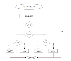 Figure 12-Perturb and Observe Algorithm for PV panels
6. Results and Discussion
6.1 Mode 1 operation
The waveforms for four switches, voltage at primary side vp, the evolution of load voltage and power are shown below.
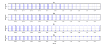 Figure 13- Waveforms for each switch in Mode 1.
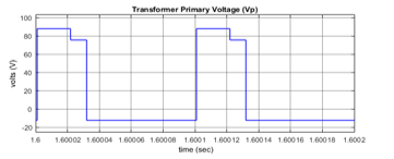 Figure 14-Primary Voltage in Mode 1
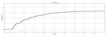 Figure 15- Load voltage curve for mode 1
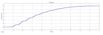 Figure 16-Load power curve for mode 1
As apparent from Figure 13, the switches SA1 and SA2 work on the complementary signal and likewise switches SB1 and SB2 operate on complementary drive signal. Similarly in Figure 14, primary voltage of the transformer is shown. After 1.6 second, the system response can be deemed as steady state response, in which during the first two states, primary voltage across the transformer is positive, while it is negative in the remaining two states, while the total area under the waveform is zero. This is expected, after all; the transformer can forward only alternating voltage across its winding. The three different levels of voltage Vp correspond to each state of the converter in each of which Vp depends on the topology of the converter.
6.2 Mode 2 operation
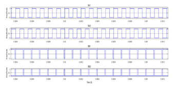 Figure 17-Waveforms for each switch in Mode 2
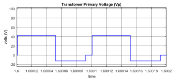 Figure 18- Primary Voltage in Mode 2
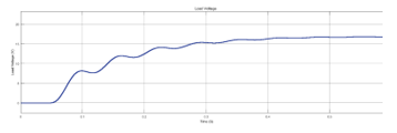 Figure 19- Load Voltage in Mode 2
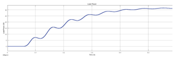 Figure 20- Load Power in Mode 2
The switch waveforms for operation in Mode 2 are shown in Figure 17. Similarly, in Figure 18, the transformer primary voltage Vp is shown. The three different steps in the Vp represent different stages of the transformer. Since in the beginning, Vp equal Vpv, hence the first step in the waveform is higher. In the second step, the voltage is below zero because the transformer must balance the voltages to keep its core from saturation. In the third step, the transformer voltage becomes zero, and it gets the time to reset itself. In case of load voltage and power, it can be seen that voltage rises from zero in transient response and stabilizes itself to a value of around 17 V.
6.3 Mode 3 Operation
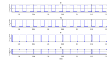 Figure 21- Waveforms for each switch in Mode 3
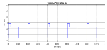 Figure 22- Primary Voltage in Mode 3
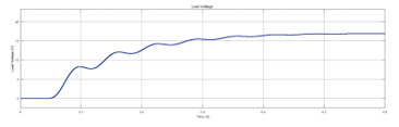 Figure 23-Load Voltage in Mode 3
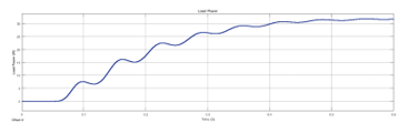 Figure 24- Load power in Mode 3
Similar to the previous two modes, in mode 3 operation, switch waveforms for each pair work in complementary mode, while Figure 22 corresponds to the transformer primary waveform. Each step represents a different mode of the converter, which were discussed previously. Most importantly, if the transformer voltage is positive for some time period, it should be negative for some other time period, in order to avoid saturation of the core.
7. Conclusion
In this paper, full bridge three port converter is discussed. Based on the standard design of full-bridge converter, we have modeled and derived a three port converter. The presented method splits the two switching legs of the full bridge converter into two switching cells with different sources. The presented converters offer the advantages of simple topologies and control, reduced number of devices, and a single-stage power conversion between any of the three ports. They are suitable for renewable power systems that are sourced by solar cells or wind turbines, etc.
The converter can operate in three different modes including Single Input Single Output, Single Input Dual Output and Dual Input Single Output. The operation in each of these modes depends on the conditions at hand, for example, the intensity of sunlight and load demand etc. We have analyzed the state equations, inductor volt-second balance and capacitor charge balance for each state.
Additionally, we have analyzed the Zero-Voltage Switching mechanism in the modeled converter. The transformer inductances such as leakage inductance and magnetizing inductance play crucial role in enabling ZVS mode in the presented converter. Furthermore, we have discussed the PV panel in detail which is the primary source of power in the converter. The PV panel incorporates standard PV cells made of silicon, along with Maximum Power Point Tracker (MPPT) which includes a buck-boost converter with a separate controller to keep the operation of the cells to produce maximum power at the output.
The input to the PV panel includes three parameter to select the mode of operation. We have also discussed the control algorithm called Perturb and Observe for keeping the maximum power. The results of the converters for each of the mode of operation are produced and discussed. These include the key waveforms of switches present in the converter, the voltage at the primary winding of the transformer, output voltage and power waveforms. The variation of the primary voltage during each state is rationalized.
- J. AL-Chlaihawi, A. Craciunescu and A. G. Al-Gizi, “Power Flow Management in Three Port Converter Using PV Panel with Maximum Power Point Tracker,” 2017 10th IEEE International Symposium on Advanced Topics in Electrical Engineering (ATEE 2017), Bucharest, Romania, March 23-25, 2017, pp.585-590, doi:10.1109/ATEE.2017.7905136.
- D. Napoli, F. Crescimbini, L. Solero, F. Caricchi and F. G. Capponi, “Multiple-input DC–DC power converter for power-flow management in Hyrbid Vehicles,” Proceedings of IEEE Industrial Applications Conference, pp. 1578-1585, 2002.
- Tao, A. Kotsopoulos, J. Duarte and M. Hendrix, “Transformer-coupled multiport ZVS bidirectional dc-dc converter with wide input range,” IEEE Transactions on Power Electronics, vol. 23, no. 2, pp. 771-781, 2008.
- Xu, C. Zhao and H. Fan, “A PWM plus phase-shift control bidirectional dc-dc converter,” IEEE Transaction on Power Electronics , vol. 19, no. 5, pp. 666-671, 2004.
- Qian, O. Abdel-Rahman, H. Al-Atrash and I. Batarseh, “Modeling and Control of Three-Port DC/DC Converter Interface for Satellite Applications,” IEEE TRANSACTIONS ON POWER ELECTRONICS, vol. 25, no. 3, pp. 637-649, 2010.
- Al-Chlaihawi1, A. Al-Gizi. and A. Craciunescu, “The Analysis and Comparison of Multiport Converter used for Renewable Energy Sources,” Advances in Science, Technology and Engineering Systems Journal (ASTESJ), vol. 2, no. 3, pp. 906-912, 2017.
- W. Erickson and D. Maksimovic, “Converter Circuits,” in Fundamentals of Power Electronics, New York, KLUWER ACADEMIC PUBLISHERS, 2001.
- Wu, K. Sun, R. Chen and H. Hu, “Full-Bridge Three-Port Converters With Wide Input Voltage Range for Renewable Power Systems,” IEEE TRANSACTIONS ON POWER ELECTRONICS, vol. 27, no. 9, 2012.
- L. FLOREA and A. BĂLTĂTANU, “Modeling Photovoltaic Arrays with MPPT Perturb & Observe Algorithm,” in The 8th international symposium on advanced topics in electrical engineering (ATEE), Bucharest, Romania, 2013.