Co-designed accelerator for homomorphic encryption applications
Volume 3, Issue 1, Page No 426–433, 2018
Adv. Sci. Technol. Eng. Syst. J. 3(1), 426–433 (2018);
 DOI: 10.25046/aj030152
Keywords: Homomorphic encryption, Hardware accelerator, Modular polynomial multiplication, High Level Synthesis
Fully Homomorphic Encryption (FHE) is considered as a key cryptographic tool in building a secure cloud computing environment since it allows computing arbitrary functions directly on encrypted data. However, existing FHE implementations remain impractical due to very high time and resource costs. These costs are essentially due to the computationally intensive modular polynomial multiplication. In this paper, we present a software/hardware co-designed modular polynomial multiplier in order to accelerate homomorphic schemes. The hardware part is implemented through a High-Level Synthesis (HLS) flow. Experimental results show competitive latencies when compared with hand-made designs, while maintaining large advantages on resources. Moreover, we show that our high-level description can be easily configured with different parameters and very large sizes in negligible time, generating new designs for numerous applications.
1. Introduction
This paper is an extension of the work originally presented in 2017 IEEE International Symposium on Design and Diagnostics of Electronic Circuits and Systems [1].
Homomorphic encryption is one of the most significant advances in cryptography in the last decade. It allows arbitrary computations on ciphertexts without compromising the content of the corresponding plaintexts. Thus, data can remain confidential while it is processed, enabling useful tasks to be accomplished with data being stored in untrusted environments. Considering the recent growth in the adoption of the cloud computing and the large deployment of the internet of things, homomorphic cryptography will have a major impact on preserving security and privacy in the coming years. Enterprise customers in the medical and financial sectors, for example, can potentially save money and streamline business processes by outsourcing not only the storage but also the computation of their data to public clouds.
Since the introduction of the first fully homomorphic encryption (FHE) scheme by Gentry [2] in 2009, we have noticed substantial research in the area, for the purpose of designing new homomorphic encryption algorithms, improving the schemes, their implementations, and their applications. Among them, the schemes that are based on Ring Learning With Errors (RLWE) [3] [4] [5] are among the most efficient homomorphic schemes because of their simpler structure, strong hardness assumptions, reduced key size, and reduced ciphertexts expansion with respect to previous schemes. Many of these RLWE-based schemes have been implemented in software [6] [7] [8] [9]. Results report very large latencies and resources consumption. So, in order to improve the performance of homomorphic encryption schemes, there has been research into the hardware acceleration of various homomorphic schemes and their building blocks. To date, there have been few hardware implementations for cryptosystems based on the RLWE problem. The corresponding architectures were mainly designed for fixed and small length operands and optimized for a restricted set of parameters [10], [11], [12], making them limited in terms of target applications and security requirements.
This paper presents a flexible and configurable accelerator implementing modular polynomial multiplication; the main performance bottleneck in RLWE-based homomorphic schemes. The work describes a software/hardware (SW/HW) co-designed architecture based on a High-Level Synthesis (HLS) approach. By combining HLS and SW/HW partitioning, we are able to easily configure our modular multiplier with large parameters (larger than those seen in the literature) suited for high security requirements. In addition, our modular polynomial reducer can be defined as any generic (cyclotomic) polynomial, allowing optimizations in the homomorphic context. We demonstrate the efficiency of the approach on many designs of full modular polynomial multipliers satisfying different area/latency trade-offs. So, our results can guide a designer in his choice of the appropriated configuration with respect to the targeted application.
The paper is organized as follows. In section 2, the background information is introduced. Section 3 presents the related works. Section 4 describes our proposed design. Implementation details are reported and discussed in section 5.
2. Theoretical background
2.1. Homomorphic encryption
The purpose of homomorphic encryption is allowing computations on encrypted data. This means that if a user has a function called and wants to get for some plaintext messages , it is possible to instead compute on the corresponding ciphertexts obtaining a result which decrypts to .
Formally, if then when evaluating a function homomorphically on , we get:
Since every function can be expressed as a series of additions and multiplications over some algebraic structure, a homomorphic encryption scheme can be defined as an augmented encryption scheme with two additional functions HE.Add() and HE.Mult() to add or multiply on ciphertexts, that result in a ciphertext encrypting respectively the sum or the product of the underlying plaintexts. Figure 1 shows an example of application of FHE in the context of cloud computing. When the number of successive additions HE.Add() and multiplications HE.Mult() can be unlimited during the evaluation step (i.e., computation of the function f), the scheme is known as a fully homomorphic encryption scheme. This generally requires to periodically refresh the ciphertext, otherwise it will be impossible to decrypt. This operation is performed in the encrypted domain and is called “bootstrapping”.
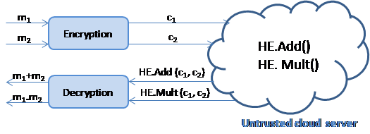 Figure 1. Homomorphic encryption in the context of cloud computing
2.2. Analysis of software implementations of homomorphic schemes
In order to define the most frequent and time consuming functions during the execution of homomorphic encryption schemes, we profiled existing software implementations [6] [8] of three RLWE-based cryptosystems. Figure 2 shows the profiling results. The analysis reports that polynomial multiplication consumes 41% to 58% of the total execution time. The polynomial multiplication is needed in the encryption, decryption, and evaluation (homomorphic multiplication) steps, as well. For instance, we resume in Figure 3 the operation flow of homomorphic multiplication of two ciphertexts (c1, c2) in case of scheme 2 (see Figure 2). In practice, we need 4 polynomial multiplications in order to get cmult. For this reason, a hardware acceleration of this function is of great interest. Hence, an optimized implementation of the modular polynomial multiplication is the target of this paper.
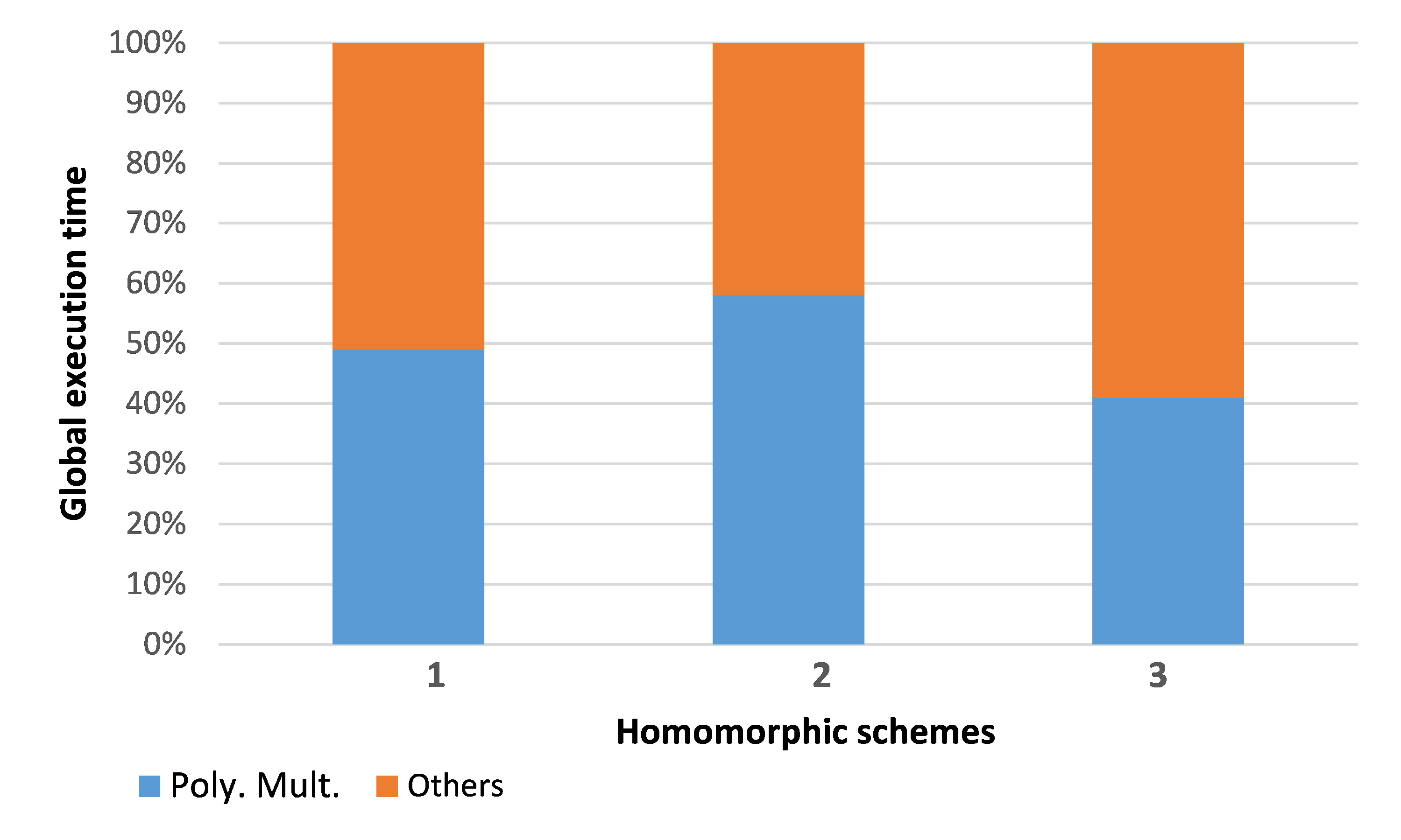 Figure 2. Profiling results of existing software implementations of three RLWE-based homomorphic schemes
 Figure 3. Homomorphic multiplication of two ciphertexts
2.3. Modular polynomial multiplication in RLWE-based schemes
In RLWE-based cryptosystems, the primitives are defined over a modular polynomial ring of the form where is a specific irreducible polynomial (cyclotomic polynomial) of degree n and q is an integer modulus ( . Parameters n and q define respectively the degree and the coefficient size of polynomials in . Operating in requires reductions modulo q and modulo .
Let and be two polynomials of . Computing in needs to first compute the polynomial multiplication of and and then reduce the result modulo .
Here is a simple example where , and . We choose:
As shown in figure 4, the result mod is equal to .
2.4. Parameters Derivation
The schemes based on the RLWE problem are governed by a number of inter-related parameters. The modulus q and the degree n are chosen in order to satisfy a given security level and a given multiplicative depth L (defined as the maximal number of multiplications that the scheme can handle before it becomes necessary to apply the bootstrapping procedure). The derivation of these parameters is getting increasing attention lately, in order to provide easy-to-use guidelines for real world applications. In a nutshell, the methodology for parameters extraction aims at sizing these parameters in order to respond to the desired trade-off between security, efficiency, and correctness. Real use-cases of homomorphic cryptosystems define requirements for the multiplicative depth L and the security level λ, then one needs to choose the corresponding values of n and q. Figure 5 illustrates the wide space of practical parameters for RLWE-based schemes with different constraints on L. These configurations are extracted from [6] where the authors explain how to choose these parameters in order to guarantee correctness and security against lattice attacks. They use a lattice basis reduction algorithm based on the van de Pol and Smart approach. This algorithm determines an upper bound on the modulus in a given dimension and for targeted numbers of multiplicative depth L, to ensure a given security level.
For example, with L set to 1, polynomials with a degree around 1024 and coefficients on less than 100 bits can be sufficient. But another scheme requires at least a degree n = 101853 and a coefficients size = 278 bits to achieve a security level λ = 80 bits and a multiplicative depth of 20. Consequently, if we want to target a large set of real applications, our design must be flexible and accept such variations of the parameters.
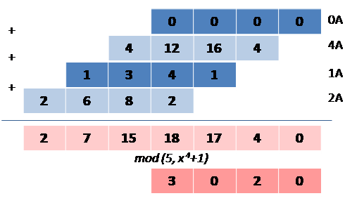 Figure 4. Example of modular polynomial multiplication in Rq
3. Related works
Two principal ways are employed in order to accelerate homomorphic cryptosystems: hardware implementation and GPU (Graphic Processing Unit) acceleration. Hardware accelerators focus mainly on accelerating the most complex functions of homomorphic encryption schemes. There has been some research already conducted into hardware implementations of RLWE-based schemes and their related building blocks. Almost all of them focus on the polynomial multiplication.
Many of these implementations have used the Number Theoretic Transform (NTT) or the Negative Wrapped Convolution (NWC) to perform polynomial multiplication in Rq efficiently. NTT and NWC are two special forms of the Fast Fourier Transform (FFT), known as the asymptotically fastest algorithm for computing polynomial multiplication.
In [10], Doröz et al. propose an implementation of the modular polynomial multiplication computed with the NTT algorithm and a Barrett reducer. A pre-computation based on the Chinese Remainder Theorem (CRT) is performed on input polynomials to reduce the size of coefficients. The overall architecture is based on an array of units, which gives some flexibility to process several residue polynomials in parallel. They evaluate their architecture on polynomials of fixed degree n = , and fixed coefficients size bits. Their accelerator was dedicated for a specific homomorphic scheme. In [11], Chen et al. present an optimized design of the modular polynomial multiplication.
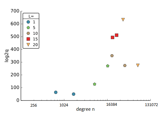 Figure 5. Examples of concrete parameters (degree, coefficients size, multiplicative depth) of some RLWE-based schemes
All computations are carried out in the FFT domain on polynomials with degree n [256, 2048] and coefficients size [20, 29]. They provide a selection method for the parameter set supporting efficient modular reduction, meeting at the same time the security requirements for RLWE and Somewhat Homomorphic Encryption (SHE) schemes. SHE means that the maximum number of successive operations in the encrypted domain is limited. Though efficient, this selection leads to many restrictions on the polynomials supported by the design: polynomial modular reduction is in fact computed with respect to the common choice When FFT multiplication using NWC is employed, they show that the modular reduction is eliminated; this elimination comes at the expense of pre- and post-computation steps. A hardware architecture for the modular polynomial multiplication is described in [13]. They provide a fast unit for polynomial operations using CRT and NTT for multiplication combined with an optimized memory access scheme and a Barrett reduction method. The implemented unit can be used to instantiate a specific encryption scheme. Results are provided for n = 32768 and = 1228 bits. The authors of [14] use the Karatsuba algorithm to implement the modular polynomial multiplication in hardware. They demonstrate that for various degrees and coefficient sizes, Karatsuba can be a good alternative to FFT. Lastly, Jayet-Griffon et al. [12] consider the polynomial multiplication of 512-degree polynomials with 32-bit coefficients. They analyze and compare three algorithms (Karatsuba, FFT, and Schoolbook): the Schoolbook method is shown as the most efficient for a hardware implementation, due to its simple and regular structure. Modular reductions were not covered in their work.
All the aforementioned related works reported significant speed up factors when compared with software implementations. This speed up illustrates that further research into hardware implementations could greatly improve the performance of FHE schemes. However, they are almost all designed for fixed length operands and optimized for one specific type of multiplication algorithm (mainly FFT-based algorithms) which puts restrictions on the parameters selection. This makes them limited to some specific schemes and application domains. Besides, the operand sizes are not very large, which has a direct impact on the security level of the cryptosystem. When modular polynomial reductions are performed, the simplest (and more limiting) choice is often selected.
Consequently, existing designs can be considered as proof-of-concept implementations only suitable for homomorphic encryption with small multiplicative depth circuits and low computation complexity. In the homomorphic context and because of its rapid growth evolution, new designs with a wide range of parameters are needed. These parameters are very large, consume large amounts of memory, and require many resources in order to perform efficient computations. Thus, memory storage and available resources in a target device should be taken into consideration, especially when manufacturing a specific circuit is not affordable and FPGA (Field Programmable Gate Array) platforms are therefore intended.
4. Software/Hardware design description
4.1. General presentation
We propose a hybrid and flexible SW/HW design based on a generic polynomial multiplier. This design is basically constructed from two parts: a dedicated hardware accelerator, and the software running on a general-purpose processor. Our solution aims at improving the overall performance and supporting much larger parameter sets than previous designs while optimizing resources for a given computation performance level. As in most previously published approaches, we will demonstrate our solution on FPGA-based implementations. However, the same approach may also be used with pre-characterized libraries to generate an application-specific integrated circuit (ASIC). The general-purpose processor can be implemented on-chip, or the hardware part of the accelerator can be connected to a computer. The interface between hardware and software can thus be performed, for example, through a high performance AXI (Advanced eXtensible Interface) bus, when software is running on an embedded processor, or a PCI (Peripheral Component Interconnect) express bus in the case of a computer processor. The choice should take into account the performance targeted for the global design, the communication and post-processing overheads, as well as the implementation constraints.
4.2. Design configurability
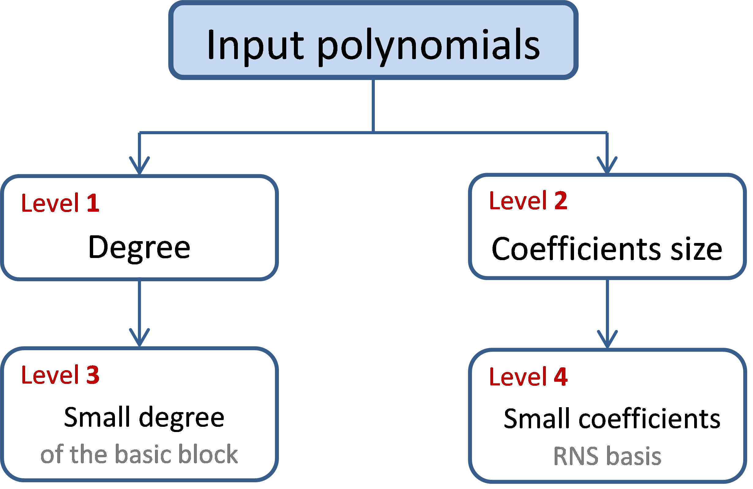
Our accelerator has been designed to support polynomials of any degree and any coefficients size. This goal has been met thanks to four hierarchy levels. As shown in Figure 6, level 1 and level 3 compute the product of two polynomials with large degree, while levels 2 and 4 deal with the product of coefficients with large sizes. This approach allows us to design efficient implementations for the lower (smaller) blocks, and configurable algorithms for the upper (larger) ones.
The designer starts by defining the input parameters (degree, coefficients size and irreducible polynomial used for the modular reduction).
In order to compute the multiplication of large input polynomials, we first represent the inputs as sets of polynomials of smaller fixed degree K. Then, we compute the pairwise products of each pair of sub-polynomials, using a hardware block for the multiplication of polynomials of fixed degree K based on the Schoolbook algorithm. This algorithm is not the fastest from a pure algorithmic point of view (asymptotic complexity), but it has three main advantages: it is more efficiently implemented on FPGA targets [12], it does not require pre- or post-processing and it does not impose any specific constraints thus allowing the possibility of optimizations such as batching (see section 5.3). An additional reason for choosing this algorithm is that the proposed decomposition limits the degree of the polynomials at level 3, so the degrees required to take full advantage of the asymptotic complexity of other algorithms is not reached.
The product of large coefficients is calculated through a RNS (Residue Number System) approach [15]. The advantage of RNS is that computations can be performed in parallel, that can result in a significant speed-up. We convert each large coefficient into a set of several values of smaller size by applying the RNS transformation. This technique can be easily made (almost) independent of the coefficient size: in order to support larger coefficients, it is sufficient to add a new element to the existing RNS basis without need to change the underlying architecture. A more detailed description of our approach is discussed in [16].
Let us mention that for small degrees and/or small coefficients sizes, level 1 and/or level 2 are optional (see Figure 6), as the algorithm can operate directly on full size operands.
4.3. SW/HW Partitioning
Our hybrid design implements part of the computations in software and part of them in hardware. The adopted partitioning is summarized in Figure 7. On the software-level, we consider simple and cheap computations such as input representations in subset polynomials, RNS basis generation, and polynomial additions; additionally, polynomial modular reduction is also computed on the main processor, in order to take advantage of the flexibility of a software implementation.
The hardware part implements the product of large coefficients in the RNS domain, and the Schoolbook multiplication algorithm at the polynomial level.
In order to reach our goals in terms of flexibility (size of parameters, but also implementation target), the hardware blocks are generated with a High Level Synthesis (HLS) tool.
4.4. High Level Synthesis
High Level Synthesis aims at transforming a generic input algorithm into a Register Transfer Level (RTL) architecture for a given target technology. This allows obtaining better productivity when compared to classical implementation approaches using direct RTL design in languages such as VHDL or Verilog, as the designer can work on a higher level language which is much easier to maintain.
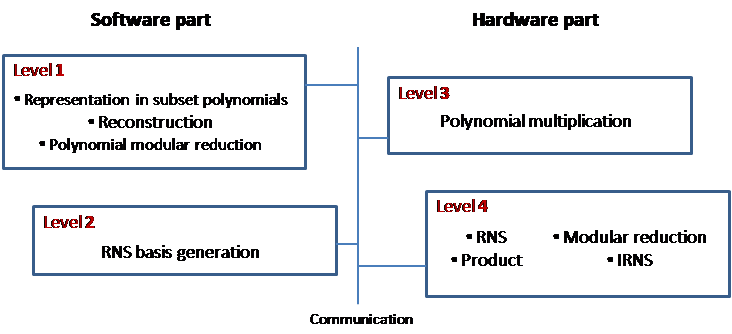 Figure 7. Modular polynomial multiplier: SW/HW partitioning overview
Several HLS tools exist; in this work, we use AUGH [17] since it is open, it may support different targets through the corresponding tool chain, and it can provide early estimations about the performance of the final result that can guide the designer in rapid refinement loops. AUGH is an autonomous HLS tool: it generates RTL descriptions quickly, under only global resource and frequency constraints [18]. This is achieved by performing incremental transformations of the input design description. The small complexity of the design space exploration (DSE) algorithm and the efficient use of all internal circuit structure constraints make this HLS tool very fast and able to generate pertinent solutions.
In this work, we will target two different FPGA technologies and a SoC (System on Chip) from Xilinx, but the methodology can be applied to other targets as well, provided that the corresponding flow is available. In our context, specifying new polynomials just implies to modify the input algorithms described in C language and let the HLS tool produce the RTL descriptions for every new specification (see Figure 8). Changing other parameters is fast and simple as well, as the designer can modify directly the high level description of the algorithm. Similar interventions on a RTL description of the design would take much more time and would be much more prone to errors due to a more complex description code.
AUGH provides different techniques for design optimizations, including unrolling and pipelining for the loops, wiring for the branch conditions and using maximum operator sharing [18]. Each RTL generation is analyzed by the user who can then command the HLS tool (with these directives) to converge towards a better solution in the next trial. DSE process detects possible transformations of the design that bring more parallelism, and applies these transformations until the user resource constraints are reached. Then, the RTL design description is generated.
5. Implementations, comparisons and discussions
5.1. Comparison with the state of the art
In order to provide a fair comparison of our results with the state of the art, we configure our design with parameters as close as possible to [10], [11] and [12] and perform the synthesis on similar targets.
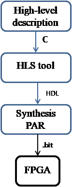 Figure 8. HLS based approach: tool chain
We set parameters for multiplication of polynomials of degree 512, 1024 and 32768 and with coefficients sizes of 26 and 32 bits. Under these configurations and for the smallest degrees, we do not divide inputs into smaller polynomials and we feed our basic block of level 3 directly with the corresponding polynomials.
Table 1 demonstrates that our approach, though about twice slower compared to manually optimized designs, consumes much fewer resources than the two designs reported in [11]. We obtain a reduction by a factor of 9 on average. This significant difference can be explained by the choice of the polynomial multiplication algorithm. For the FTT- and NTT-based algorithms (as in [11]), the pre- and post-computation steps are complex and require storing additional parameters. For the Schoolbook method, no pre- and post-computations are needed and we only have to store the input and output coefficients. Thus, FTT and NTT implementations have lower latency than our accelerator thanks to their lower complexity and their hand-crafted design but have several constraints and require a large amount of hardware resources.
For comparison with [12], where the authors implement the Schoolbook algorithm, we present two solutions in Table 2. In order to exploit parallelism and to achieve the minimal latency, we apply an optimization directive of AUGH not allowing operator sharing. Doing so, we instruct the HLS tool to use as many DSPs as possible: in this case only LUTs are used to store the coefficients and a maximum number of DSPs can be easily parallelized (first design in Table 2). In the other solution (second design in Table 2) BRAMs are used to store information, which limits the number of DSPs that can be used efficiently. It must be stressed, however, that our results are after placement and routing, while [12] only gives results after synthesis. Depending on the choice made with the HLS tool, the latency may be only slightly augmented (+28%) compared with the noticeable gain in resources (more than 35x). Resources can be further reduced up to a factor of 41 with the second solution, but leading to a loss of performance by a factor of 12.6.
For polynomials with degree 32768 used in [10], we divide the inputs into polynomials of degree 8192 and we apply our
approach first without any optimization. In this case (first design in Table 3), the hardware resources required by our design are nearly 28 times less than [10] on average; on the other hand, our design has a latency of 41 ms, while the authors of [10] report a latency of about 9.5 ms. Since our accelerator requires relatively few hardware resources, we can compute in parallel on 4 instances: with this optimization, the second design in Table 3 has a latency comparable to [10], while still maintaining a large advantage in resources.
Globally, these examples of results for our designs show that they consume fewer resources than the state of the art thanks to the proposed approach, while achieved performances can be close to hand-made designs. Using fewer resources also leads to possible parallelization of several instances while meeting the resource constraints of a given FPGA; in that case, even better performances can be reached. The approach offers at the same time a large degree of configurability, allowing the designer to change several important parameters on-the-fly. In addition, our approach is highly flexible, since the same generic high-level description can be used to produce a new circuit with different area/performance trade-offs i.e., we can generate a very cheap (but slow) polynomial multiplier, or a fast but more resource consuming one. Other possible optimizations can be applied, as it will be shown in the next sections.
5.1. Design space exploration
With our flexible design, we can instantiate our architecture with different coefficients size and different degrees, targeting several platforms. Larger parameters imply large values of n and q that grant high security levels and significant multiplicative depths.
When we handle large coefficients, our approach proposes to transform them into their respective RNS representation. The choice of the RNS basis (size and co-prime modulus) is primarily based on the coefficients size of the input polynomials and the available resources on the target device. The key idea is to take advantage of the parallelism offered by the RNS representation and speed up our computations. If we ever need to increase the supported size, it is sufficient to extend the RNS basis without need to change the underlying architecture.
The RNS basis size and modulus are kept as parameters as well as the degree K of the basic block performing the Schoolbook multiplication. Let us now fix for example the coefficients size at 64 bits and vary the degree from 8192 to 32768 to cover a new range of parameters. For each degree, we choose a different degree K of the basic block. When the resources of our target are sufficient, we perform computations in parallel on several instances.
Figure 9 shows that some configurations are more efficient than others. In fact, when computations are running on P instances in parallel, we roughly multiply the resources by P and divide the latency by P (illustrated by the cases of n=8192 and n=32768, figure 9). But, setting for example K=1024 to calculate the multiplication of polynomials with a degree 16384 is not an appropriate configuration. The performance loss is essentially due to 16² calls to the basic block Polynomial_K. When changing K and/or applying an optimization, the latency is also affected by the cost of the data transfers and therefore some configurations are not suitable.
Table 1. Comparison on Spartan 6 with polynomials of degree 1024 and 26-bit coefficients
| References | Resources | ||||
| Slice LUT | Slice Register | DSP | BRAM | Latency | |
| [11](1) | 10801 | 3176 | 0 | 0 | 40.98 |
| [11](2) | 2464 | 915 | 16 | 14 | 32.28 |
| Our work | 182 | 114 | 3 | 10 | 69.1 |
(1) Multipliers are built by pure LUTs (2) Use DSPs and Brams
Table 2.Comparison on Virtex 7 with polynomials of degree 512 and 32-bit coefficients
| References | Resources | ||||
| Slice LUT | Slice Register | DSP | BRAM | Latency | |
| [12]* | 252341 | 130826 | 512 | 2048 | 4.11 |
| Our work (1) | 7032 | 920 | 368 | 0 | 5.27 |
| Our work (2) | 171 | 102 | 3 | 3 | 66.41 |
(1) Data is stored in Lutrams (2) Data is stored in Brams *Synthesis results
Table 3.Comparison on Virtex7 with polynomials of degree 32786 and 32-bit coefficients
| References | Resources | ||||
| Slice LUT | Slice Register | DSP | BRAM | Latency | |
| [10] | 219192 | 90789 | 139 | 768 | |
| Our work (1) | 3392 | 1920 | 48 | 792 | |
| Our work (2) | 13568 | 7680 | 192 | 792 | |
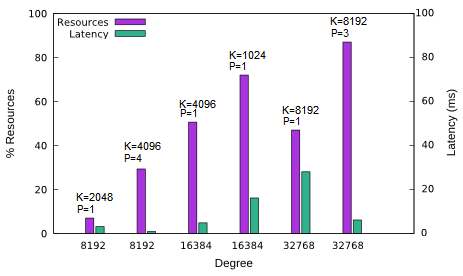 Figure 9. Performance of our designs on polynomials with 64-bit coefficients and different configurations (degree K, parallelization, degree P)
Several multipliers with different area/performance ratios can be generated by modifying the RNS basis and the degree K of the basic block, and also by the parallelization of the computations on many instances of the basic block. Thanks to the HLS design flow, rapid feedback on circuit characteristics is used to evaluate deep architectural changes in short time and pick up the more suitable parameter sets. Then, the designer can select the design satisfying his constraints among the set of generated circuits. The development timeline of a new solution is about 3 hours on average, which is a very short time in comparison with a hand-made design.
5.2. Our system performances
In this section, we evaluate the performance of our hybrid modular polynomial multiplier with respect to the communication times between hardware and software. We run computations on polynomials of degree 512 with 32-bit coefficients and we pick two choices for the modular polynomial: , and a general cyclotomic polynomial of degree 512. This choice is motivated by the possibility, allowed by a generic polynomial, of applying the batching optimization [19].This technique can be used in order to pack multiple messages into one single ciphertext, therefore allowing parallel homomorphic evaluations. Hence, it permits great versatility in the computations and improves performance. This technique is based on the CRT theorem and requires that the polynomial f(x) is different from .
To transfer data, we consider an AXI interconnection between the hardware and software part. Our platform is the Zybo Zynq-7000. In our case, we send to the FPGA two input polynomials of 32*512 bits each and we receive one polynomial of 73*1024 bits. We use one high performance AXI bus to send the input coefficients and two high performance AXI buses to receive the output polynomials: this is due to the fact that the polynomial reduction is made in software, and the multiplication result is thus (almost) twice larger than the operands. With this solution, we can enhance the performance of our system and have the final result faster: a speed up factor of about 2.98 is obtained compared with a solution with only one bus, as the hardware acceleration is mitigated by the data transfers.
Our architecture reports a global latency, including transfers, of 0.75 ms when and of 1.89 ms when has a general form, which is still very fast compared to pure software implementations.
When compared with the state of the art, we have shown that our implementations consume few resources but report smaller speed-up factors. To counter this, we have proposed to run computations on many instances of the basic block in parallel. Figure 10 illustrates an optimized proposition when performing computations on 4 instances of blocks with degree 512 in parallel.
5.3. System evaluation on larger parameters
In this section, we evaluate our approach on designs with larger parameters. For each configuration, we choose two forms of the irreducible polynomial f(x). The first one corresponds to the popular choice . The second one has a general form and allows optimizations in the homomorphic context. Tables 4 and 5 provide implementation results and comparisons with software implementations we developed with Sage and run on a Intel Core i5-2450M (2.5 GHz). We decided to make such a comparison in order to get the same parameters configuration of parameters and because published works do not cover such parameters. Our reference embedded platform (the Zybo board) has processing power and memory that are not even comparable to desktop or server CPUs. Nonetheless, and withstanding the overhead of the data transfers through the AXI bus, the results obtained are quite interesting.
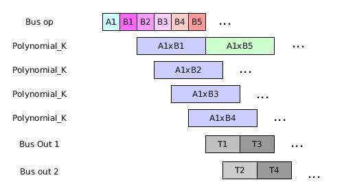 Figure 10. Parallelization of the computations on many instances of the basic block Polynomial_K [1].
Table 4. Implementation results (ms) when f(x) =
| n | q | Software implementation | Our design |
| 4096 | 32 | 32.6 | 2.1 |
| 8192 | 64 | 76.7 | 5.8 |
| 16384 | 128 | 162.8 | 11.7 |
Table 5. Implementation results (ms) when f(x) has a general form
| n | q | Software implementation | Our design |
| 4096 | 32 | 41.8 | 4.1 |
| 8192 | 64 | 88.5 | 12.7 |
| 16384 | 128 | 202.9 | 21.8 |
Results show that our approach reports significant speed-up factors when compared with pure software implementations, in spite of the large parameter values. The latencies when the polynomial reduction is computed modulo are better than the reduction modulo a polynomial with general form. This is due to the complex form of the polynomial in the second case (only 2 coefficients vs. (n+1) coefficients) and to the number of iterations required to get the final results. For a fair comparison, it must be stated that such a general form is not covered by most works in the literature, especially when hardware implementations are considered.
Several software implementations and libraries dedicated to homomorphic cryptography exist today [20], Error! Reference source not found.[21], which achieve very interesting performance when executing on high-end processors. These implementations are usually based on the NTT-based algorithm in order to speed up the modular multiplication on very large operands. This algorithm, however, has very large requirements in terms of memory usage, it constrains the choice of parameters, and it is usually optimized by exploiting the advanced instruction set available on modern processors, such as SSE and AVX. When targeting limited devices and/or current client-server frameworks, those implementations cannot be used directly because of the memory cost, or do not perform well enough due to missing advanced instructions. For this reason, a comparison with these works is difficult, since different application domains and platforms are targeted.
6. Conclusion and future works
We present a flexible and generic SW/HW co-design for the modular polynomial multiplication, the most computationally intensive operation in homomorphic cryptosystems based on the RLWE problem. Given the large parameters required in such schemes, we propose an RNS based algorithm and an efficient decomposition of the large input polynomials. Our design can be easily configured thanks to a HLS approach and sets no restrictions on the parameters that define the RLWE problem leading to high security levels and large multiplicative depths when necessary. Our approach can also optimize the accelerator for applications requiring small parameters. Our architecture can be instantiated to accelerate any RLWE-based scheme; additionally, even if the proposed methodology has been illustrated only on the polynomial multiplication, it can be used to implement and accelerate other primitives required by homomorphic schemes.
Future works include more complex communication schemes, such as using two AXI High Performance input ports and thus increase the number of instances performing in parallel. As the memory is one major bottleneck, we can reduce the amount of memory by controlling and scheduling the loading of sub-polynomials and . It may also be interesting to evaluate the benefits of a hardware implementation of the polynomial reduction. Other primitives used in the FHE schemes may also be implemented in hardware using the same methodology. Finally, these accelerators will be integrated to evaluate a full homomorphic scheme on an FPGA/processor platform targeting embedded applications, and the performance will be compared to state-of-art software libraries ported to the same environment.
- Mkhinini, P. Maistri, R. Leveugle and R. Tourki, HLS design of a hardware accelerator for Homomorphic Encryption, IEEE 20th International Symposium on Design and Diagnostics of Electronic Circuits & Systems (DDECS’17), pp. 178-183, Dresden, Allemagne, 19 au 21 avril 2017.
- Gentry, A fully homomorphic encryption scheme, Ph.D. dissertation Stanford University, 2009.
- Joppe W. Bos, Kristin Lauter, Jake Loftus, and Michael Naehrig. Improved security for a ring-based fully homomorphic encryption scheme. In Martijn Stam, editor, Cryptography and Coding, volume 8308 of LNCS, pages 45–64. Springer Berlin Heidelberg, 2013.
- Junfeng Fan and Frederik Vercauteren. Somewhat practical fully homomorphic encryption. Cryptology ePrint Archive, Report 2012/144, 2012. http://eprint.iacr.org/.
- Zvika Brakerski, Craig Gentry, and Vinod Vaikuntanathan. (leveled) fully homomorphic encryption without bootstrapping. In ITCS 2012, pages 309–325, Cambridge, Massachusetts, 2012. ACM.
- Tancrède Lepoint and Michael Naehrig. A comparison of the homomorphic encryption schemes FV and YASHE. In Progress in Cryptology – AFRICACRYPT 2014,7th International Conference on Cryptology in Africa, Marrakesh, Morocco, May 28-30, 2014. Proceedings, pages 318-335, 2014.
- Zvika Brakerski. Fully homomorphic encryption without modulus switching from classical GapSVP. In Advances in Cryptology – Crypto 2012, volume 7417 of LNCS, pages 868–886. Springer, 2012.
- Shai Halevi and Victor Shoup. Algorithms in helib. In Advances in Cryptology-CRYPTO 2014 – 34th Annual Cryptology Conference, Santa Barbara, CA, USA, August 17-21, 2014, Proceedings, Part I, pages 554-571, 2014.
- Kim Laine and Rachel Player. Simple encrypted arithmetic library – seal (v2.0). Technical report, Microsoft Research, September 2016.
- Doröz, E. Öztürk, E. Savas, B. Sunar , “Accelerating LTV Based Homomorphic Encryption in Reconfigurable Hardware”,CHES ‘15, 185-204.
- D. Chen, N. Mentens, F. Vercauteren, S. S. Roy, R. C. C. Cheung, D. Pao, and I. Verbauwhede, “High-speed polynomial multiplication architecture for ring-lwe and SHE cryptosystems,” IEEE Trans. on Circuits and Systems, vol. 62-I, no. 1, pp. 157–166, 2015.
- Cedric Jayet-Griffon, M.A Cornelie, P. Maistri, Ph. Elbaz-Vincent and R. Leveugle. Polynomial Multipliers for Fully Homomorphic Encryption on FPGA. In 2015 International Conference on ReConFigurable Computing and FPGAs (ReConFig), Mexico City, 2015, pages 1-6.
- Sinha Roy, K. Järvinen, F. Vercauteren, V. Dimitrov, and I. Verbauwhede, Modular hardware architecture for somewhat homomorphic function evaluation, in Proc. of Cryptographic Hardware and Embedded Systems – CHES 2015. Springer, pp. 164–184.
- Migliore; M. Mendez Real, V. Lapotre, A. Tisserand, C. Fontaine, G. Gogniat. Hardware/Software co-Design of an Accelerator for FV Homomorphic Encryption Scheme using Karatsuba Algorithm. In IEEE Transactions on Computers, vol.PP, no.99, pp.1-1.
- L. Garner, The residue number system, IRE Transactions on Electronic Computers, vol. EC-8, no. 2, pp. 140–147, Jun. 1959.
- Mkhinini, P. Maistri, R. Leveugle, R.Tourki and M. Machhout, A Flexible RNS based Large Polynomial Multiplier for Fully Homomorphic Encryption, 11th IEEE International Design & Test Symposium (IDT), Hammamet, Tunisia, December 18-20, 2016, pp. 131-136.
- Prost-Boucle, “Augh project” 2016, [Online]. Available: http://tima.imag.fr/sls/research-projects/augh/
- Prost-Boucle, O. Muller, and F. Rousseau, Fast and standalone design space exploration for high-level synthesis under resource constraints, Journal of Systems Architecture, vol. 60, n. 1, 79–93, 2014.
- P. Smart, F. Vercauteren, Fully homomorphic SIMD operations, Des. Codes Cryptography 71(1): 57-81 (2014).
- Seal : Simple Encrypted Arithmetic Library, https://sealcrypto.codeplex.com/
- Helib library, https://github.com/shaih/HElib
- NFLlib library, https://github.com/CryptoExperts/FV-NFLlib
- Dimitris Ziouzios, Pavlos Kilintzis, Nikolaos Baras, Minas Dasygenis, "A Survey of FPGA Robotics Applications in the Period 2010 – 2019", Advances in Science, Technology and Engineering Systems Journal, vol. 6, no. 3, pp. 385–408, 2021. doi: 10.25046/aj060344
- Peter Arato, Gyorgy Racz, "A Method for Generating, Evaluating and Comparing Various System-level Synthesis Results in Designing Multiprocessor Architectures", Advances in Science, Technology and Engineering Systems Journal, vol. 3, no. 3, pp. 129–141, 2018. doi: 10.25046/aj030318
- Eleni Bougioukou, Nikolaos Toulgaridis, Maria Varsamou, Theodore Antonakopoulos, "Hardware Acceleration on Cloud Services: The use of Restricted Boltzmann Machines on Handwritten Digits Recognition", Advances in Science, Technology and Engineering Systems Journal, vol. 3, no. 1, pp. 483–495, 2018. doi: 10.25046/aj030159

