A High Efficiency Ultra Thin (1.8 um) CdS/CdTe p-i-n Solar Cell with CdTe and Si as BSF layer

Adv. Sci. Technol. Eng. Syst. J. 3(1), 213–217 (2018);
 DOI: 10.25046/aj030125
CdTe-based photovoltaic (PV) cells provide the lowest EBPT (energy payback time) and emit less amount of GHG (green house gases) among different types of PV cells. Thus, it is very essential to enhance the efficiency of CdTe-based solar cells. A high efficiency CdTe/CdS p-i-n heterostructure solar cell is designed and the performance of the cell is investigated. All the simulations have been done using AMPS 1D (Analysis of Microelectronic and Photonic Structures) simulator. The cell consists of a transparent conducting oxide (TCO) layer (ZnO), a window layer (n-type CdS), an intrinsic layer (CdTe), an absorber layer (p-type CdTe) and a highly doped CdTe and Si as back surface field (BSF) layer. After the optimization of layer thicknesses and doping densities of different layers, we obtained a conversion efficiency of 26.01% for a total cell thickness of 1.8 um. It is also found that the conversion efficiency can be increased by simply increasing the thickness of intrinsic layer. At 1.5 AM solar irradiance, the proposed cell structure attained a Voc of 1.09 V, a Jsc of 26.78 mA/cm2, and a fill factor of 89%, reaching an overall conversion efficiency of 26.01% with CdTe as BSF layer.
1. Introduction
This paper is an extension of our previous work presented in ICAEESE 2016 [1]. The rapidly rising demand of world energy supply and the depletion of fossil fuel impose crucial challenges concerning today’s energy requirement context. It is also worth mentioning that, the surfeit burning up of fossil fuels renders threatening global warming emissions (GWE) ascribing alarming rise of terrestrial temperature while imposing serious environmental pollutions by particulate materials [2]. These aforementioned issues necessitate the blooming of alternatively dependable, affordable-cost consistent energy sources. To meet these requirements various plausible renewable energy technologies have been thriven so far. Among these alternative technologies solar photovoltaic (PV) is thought to be as one of the most potential and reliable green energy concepts that assures the direct conversion of incident solar irradiation into electrical energy. The power extracted from PV architectures is popularly being adopted and deployed in the remote areas while ensuring the minimization of electrical power transmission losses. PV power can also be potentially applied in vehicular transportation that can ensure the diminishing of global warming emissions in near future. From purely economic point of view, the flourishing market of PV is generating a shortfall in the storage of highly cost silicon wafers which takes almost 50% of the total manufacturing cost. Therefore, it fosters an opportunity for thin film solar technology to create credentials in the market of PV modules because of its moderate cost. Among different types of thin film based modules, CdS/CdTe thin-film solar cells reveals significant suitability owing to its distinctive characteristics encompassing the following aspects. Firstly, the energy bandgap of CdTe is 1.45 eV, which is favorably well-matched to the spectrum of solar radiation. It also lies in the category of direct bandgap semiconductor guiding to fairly strong light absorption with reduced generation of heat. Besides, the doping of CdTe as p-type semiconductor film as well as the formation of p-n heterojunction with the inclusion of CdS is found to be much easier. Moreover, CdS exhibits wide energy-gap of 2.4 eV and can be fabricated as n-type adopting undemanding usual techniques of film deposition [3-5]. In the meanwhile, various less-costly and manageable atomic congregation techniques have been developed for the growth of CdS/CdTe solar cells [6-7]. Also it should be mentioned that, a thickness of around 4 microns absorber layer of CdTe is almost appropriate for capturing the entire solar spectrum due to acceptable range of absorption coefficient [8-9] of CdTe (~105 cm-1) in the visible solar spectrum. All these properties of CdTe attribute to quite less material cost of the cell if compared with cells based on Si-wafers. In addition, from various respective studies, it is revealed that the energy-payback-time (average) of thin film CdS/CdTe solar cell is around 1.4 years [10] that is found to be as the rock-bottom among all PV technologies. Moreover, CdTe solar cell generates the lowest amount of GWE for per kWh electrical energy compared to other PV technologies [10].
In CdS/CdTe thin film solar cell, irrespective of superstrate or substrate configurations, light enters into the cell through the TCO and CdS (n-type) window layers. From the earlier attempts, the experimental efficiency of single junction CdS/CdTe solar cell has been reported so far around 17% [11-13]. Approximately 18.6% conversion efficiency from a CdS/CdTe solar cell incorporating complex BSF and TCO layers has been reported by Amin et al [14].
In this work, we explore the possibilities and chances of enhancing the efficiency of CdS/CdTe heterojunction solar cell with the insertion of an intrinsic layer of CdTe. Additionally, a back surface field (BSF) layer of highly doped CdTe (p+ layer) and Si (p+ layer) are sandwiched between back contact and the absorber layer of p-CdTe in order to diminish the recombination loss and thereby, magnifying the conversion efficiency. In this proposed structure as depicted in Figure 1, a TCO layer of ZnO is inserted to enhance the level of Voc by minimizing the series resistance of the cell.
2. Methodology
In this work the proposed cell is simulated in AMPS 1D simulator to optimize the layer thicknesses of TCO, window, absorber, intrinsic and BSF layers, and the doping density of BSF layer to achieve the maximum possible conversion efficiency under 1.5 AM solar irradiance. The properties of n-CdS, p-CdTe, a-Si and n-ZnO, those are given in Table 1, are taken from [13-15].
Table 1 Material Properties
| Parameters | a-Si | CdTe | CdS | ZnO |
| εr | 11.9 | 9.4 | 9.0 | 9.0 |
| μn (cm2.V-1.s-1) | 20 | 500 | 350 | 100 |
| μp(cm2.V-1.s-1) | 2 | 60 | 50 | 25 |
| Eg (eV) | 1.72 | 1.45 | 2.42 | 3.0 |
| NC (cm-3) | 2.5×10²⁰ | 8×10¹⁷ | 2.4×10¹⁸ | 2.2×10¹⁸ |
| NV (cm-3) | 2.5×10²⁰ | 1.8×10¹⁹ | 1.79×10¹⁹ | 1.8×10¹⁹ |
| χ (eV) | 3.8 | 4.28 | 4.5 | 4.35 |
3. Function of Intrinsic Layer
To comprehensively explain the function of intrinsic layer the simplified energy band diagram for thermal equilibrium condition is shown in Figure 2. It is worth mentioning that while depicting the energy band diagram, gradient of the quasi-Fermi level has not been shown for simplicity. Literally, when light falls and photo-voltage is generated it biases the p-n junction in forward bias mode and therefore the Fermi level should not be continuous throughout the junction of cell. However, it is evident from this diagram that, the inclusion of intrinsic layer increases the width of depletion layer where mainly the photons are absorbed and electron-hole pairs are generated. From Figure 2, it is clear that the generated electrons can move easily towards the TCO layer (left to n-CdS) due to the slope of electron energy and the effect of tunneling. Similarly photo-generated holes can move towards the back contact layer (right to BSF layer) due the slope of holes energy.
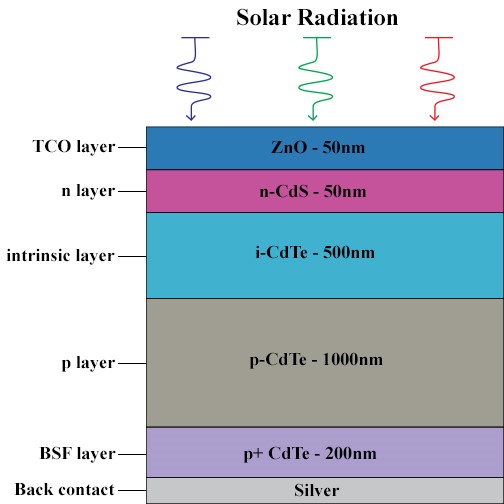 Figure 1The structure of the proposed p-i-n CdS/CdTe solar cell
4. Results and Discussion
In this work, using AMPS 1D simulator we have optimized the thickness of different layers of the cell in order to improve the efficiency. Throughout the simulation, the thicknesses of window layer (n-CdS) and absorber layer (p-CdTe) are kept constant at 50 nm and 1000 nm respectively (as shown Figure 1). We only explored the possibilities of enhancing the conversion efficiency of the cell by optimizing the thicknesses of BSF and intrinsic layers. The proposed structure is simulated in AMPS 1D environment and the I-V characteristics of the cell under 1 sun illumination is extracted from AMPS 1D simulator which is exemplarily shown in Figure 3. After simulation under different doping densities and thicknesses we obtained several figures and results from which we extracted the cell efficiency for desired doping density and thickness.
We explored the effects of doping density of p-CdTe BSF layer on the conversion efficiency for a BSF layer thickness of 50 nm and the results are shown in Figure 4. From Figure 4 it is found that beyond doping density of 2×1018 cm-3, the conversion efficiency increases exponentially. The effects of the insertion of amorphous Si (a-Si) and CdTe as BSF layer on the efficiency are also investigated.
Figure 5 and Figure 6 depict the effects of BSF layer thickness (highly doped p-Si and p-CdTe) on the conversion efficiency without the inclusion of intrinsic layer. For this analysis, the doping density of a-Si and CdTe are considered as 6.0×1017 cm-3 and 1.0×1019 cm-3 respectively . At a BSF layer thickness of 200 nm, the maximum efficiencies for a-Si and CdTe are attained to be 23.0% and 24.46% respectively. It is observed that beyond 200 nm thickness of BSF layer, in case of a-Si the efficiency becomes saturated whereas in case of CdTe the efficiency increases almost linearly. From Figure 5 and 6 it is also noticed that in the proposed CdS/CdTe solar cell, CdTe outperforms a-Si as a BSF layer.
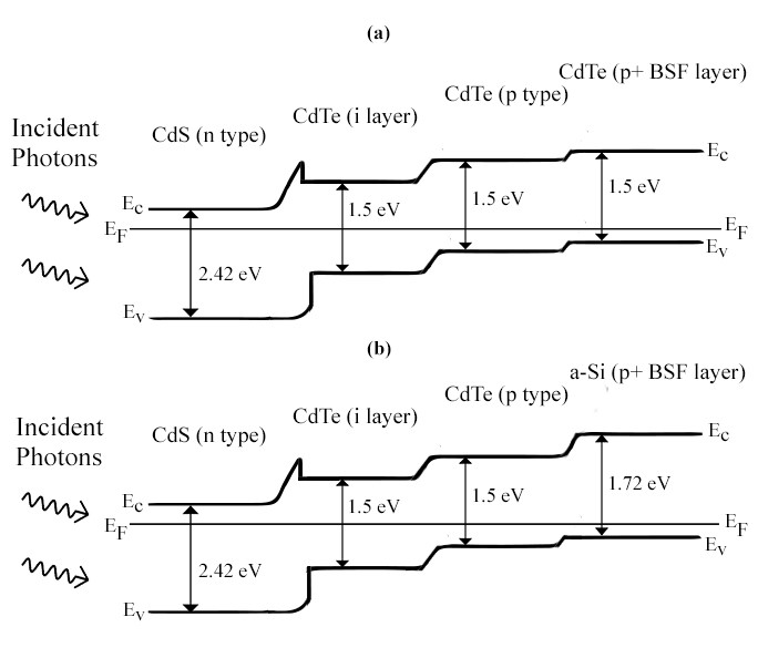 Figure 2 Simplified energy band diagram of proposed (a) p-i-n CdS/CdTe (BSF layer: CdTe) (b) p-i-n CdS/CdTe (BSF layer: a-Si) solar cells
Figure 7 and 8 show the effects of intrinsic layer (CdTe) thickness on the cell’s conversion efficiency considering a-Si and CdTe as BSF layers separately. It is observed that in both cases the conversion efficiency increases linearly with the increase of intrinsic layer thickness. However, the maximum conversion efficiency at thickness 500 nm of intrinsic layer for CdTe and a-Si (as BSF layer) are found to be 26.01% and 24.51% respectively. The dependence of short circuit currents on the variation of intrinsic layer thickness for both CdTe and a-Si as BSF layers are also studied as depicted in Figure 9. From this comparison it is realized that CdTe as BSF layer provides larger short circuit current than that of a-Si.
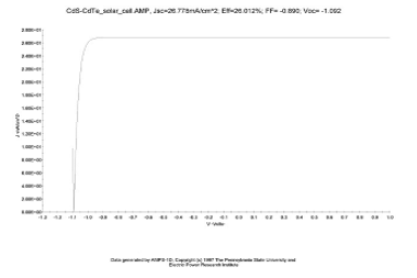 Figure 3 I-V characteristics of the proposed p-i-n CdS/CdTe solar cell.
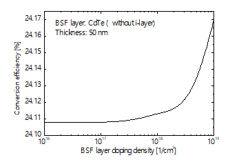 Figure 4 Effects of BSF layer doping density on the conversion efficiency
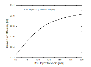 Figure 5 Effects of BSF (Silicon) layer thickness on the conversion efficiency
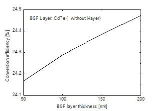 Figure 6 Effects of BSF (CdTe) layer thickness on the conversion efficiency
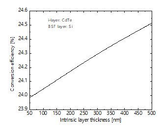 Figure 7 Effects of thickness of intrinsic layer on the conversion efficiency
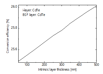 Figure 8 Effects of thickness of intrinsic layer on the conversion efficiency
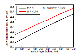 Figure 9 Comparison of current density for Si and CdTe as BSF layer
5. Conclusions
An ultrathin (1.8 mm) p-i-n CdS/CdTe PV cell is designed and simulated using 1D AMPS simulator. The thicknesses of intrinsic layer and BSF layer and the doping density of BSF layer are optimized. It is found that CdTe outperforms Si as a BSF layer. The maximum conversion efficiency of the proposed solar cell is found to be 26.01% taking CdTe as BSF layer. Simulation results revealed that a highly doped p+ CdTe layer (BSF layer) has significant contribution in achieving such a high efficiency. At 1.5 AM solar irradiance, the proposed cell structure with CdTe as BSF layer achieved an open-circuit voltage of 1.09 V, a short-circuit current density of 26.78 mA/cm2, and a fill factor of 89% and the corresponding overall conversion efficiency of 26.01%. The same structure with Si as BSF layer achieved an open-circuit voltage of 1.06 V, a short-circuit current density of 26.66 mA/cm2, and a fill factor of 87%, and the corresponding overall conversion efficiency of 24.51%. Compared to our previous work [1] the cell thickness is reduced by 30% with a sacrifice of 0.73% cell efficiency.
Conflict of Interest
The authors declare no conflict of interest.
Acknowledgment
The authors are thankful to East West University, Dhaka, Bangladesh for financial supports.
- Mofazzal Hossain, Md. Minhaz Ul Karim, S. Banik, Nahid A. Jahan and M. A. Matin, “Design of a high efficiency ultrathin CdTe/CdS p-i-n solar cell with optimized thickness and doping density of different layers,” ICAEESE, Putrajaya, Malaysia 2016, 14-16 Nov.DOI: 10.1109/ICAEES.2016.7888058
- Nishimura, Y. Hayashi, K. Tanaka, M. Hirota, S. Kato, M. Ito, K. Araki and E.J. Hu “Life cycle assessment and evaluation of energy payback time on high-concentration photovoltaic power generation system,” Applied Energy 87, pp. 2797-2807, 2010.https://doi.org/10.1016/j.apenergy.2009.08.011
- C. Morris and S. K. Das, “Some fabrication procedures for electrodeposited CdTe solar cells,” International Journal of Solar Energy, 12(1-4), pp. 95-108, 1992.http://dx.doi.org/10.1080/01425919208909753
- L Chu, “Thin film cadmium telluride solar cells by two chemical vapor deposition techniques,” Solar Cells, 23, pp. 31-48, 1988.https://doi.org/10.1016/0379-6787(88)90005-1
- Ikegami, “CdS/CdTe solar cells by screen-printing-sintering technique: Fabrication, photovoltaic properties and applications,” Solar Cells, 23(1-2), pp. 89-105, 1988.https://doi.org/10.1016/0379-6787(88)90009-9
- L Chu and S. S. Chu, “High efficiency thin film CdS/CdTe solar cells,” International Journal of Solar Energy, 12(1-4), pp. 121-132, 1992.http://dx.doi.org/10.1080/01425919208909755
- M. Nikale, S. S. Shinde, C. H. Bhosale, and K. Y. Rajpure, “Physical properties of spray deposited CdTe thin films: PEC performance,” Journal of Semiconductors, 32(3), pp. 033001-7. 2011.http://doi.org/10.1088/1674-4926/32/3/033001
- Marple, D. T. F., “Optical Absorption Edge in CdTe: Experimental,” Phys. Rev. 150(2), 728-734, 1966. https://doi.org/10.1103/PhysRev.150.728
- Kim Mitchell1, Alan L. Fahrenbruch and Richard H. Bube, “Photovoltaic determination of optical-absorption coefficient in CdTe,” J. Appl. Phys. 48, pp. 829-830, 1977. https://doi.org/10.1063/1.323636
- Jinqing Peng, Lin Lu, and Hongxing Yang, “Review of life cycle assessment of energy payback and greenhouse gas emission of solar photovoltaic systems,” Renewable and Sustainable Energy Reviews 19,255-274, 2013. https://doi.org/10.1016/j.rser.2012.11.035
- First Solar Inc (2014), http://investor.firstsolar.com/releasedetail.cfm?ReleaseID=828273
- NREL, 2001. Available in nrel.gov/news/press/2001/1501_record.html
- Britt and C. Ferekides, “Thin film CdS/CdTe solar cell with 15.8% efficiency,” Applied Physics Letters, 62(22), p. 2851-2852, 1993. https://doi.org/10.1063/1.109629
- Nowshad Amin, M A Matin, M M Aliyu, M A Alghoul, M R Karim and K Sopain, “Prospects of Back Surface Field Effect in Ultra-Thin High-Efficiency CdS/CdTe Solar Cells from Numerical Modeling,” Int. J. Photoenergy, 2010, pp. 1-8, 2010. http://dx.doi.org/10.1155/2010/578580
- Minami, Tadatsugu, “Transparent conducting oxide semiconductors for transparent electrodes,” Semiconductor Sci. and Technol. 20(4), pp. S35-S44, 2005. https://doi.org/10.1088/0268-1242/20/4/004
No related articles were found.