Control of a three-stage medium voltage solid-state transformer
 , Favio Mengatto 1, Alejandro Oliva 1, Jorge Solsona 1, German Bloch 2, Angelica Delgadillo 2
Adv. Sci. Technol. Eng. Syst. J. 2(6), 119–129 (2017);
 DOI: 10.25046/aj020615
This paper proposes the modeling and control of a Solid-State Transformer using a three-stage conversion topology. First, a rectification stage is used, where a three-phase high-voltage AC signal is converted to a DC level; this stage is then followed by a DC-DC converter, and finally an inverter is used to convert the DC into a three-phase low-voltage AC signal. The adopted topology is modeled using a simplified model for each stage, useful to design their controllers. Based on these models, the controllers are tuned to obtain a good performance to sudden load changes. This performance is tested through simulations.
1. Introduction
It is necessary to mention that this paper is an extension of work originally presented in [1]. This extension includes a detailed description of the proposed models and controllers. These models are used for tuning the controller parameters in order to obtain good performance in presence of sudden load changes.
Solid-State Transformers (SST) are emerging as a new technology capable of replacing power distribution transformers [2]. It is expected that the next generation of the power distribution transformers is based on power electronics semiconductor devices [3]. By using these semiconductors, it is possible to design an apparatus based on power converters with smaller and lighter high-frequency transformers. In this way, it is possible to obtain a smaller and lighter distribution transformer when compared with a traditional transformer of the same power rating. Roughly speaking, SSTs work as follows. In a first stage a sinusoidal signal of, typically, 50 or 60 Hz is converted to a highfrequency signal. Then, the amplitude of this signal is changed, by using a small high-frequency transformer, and finally in a third stage a new signal of the same frequency as the input signal but different amplitude is obtained.
Several topologies for the SST can be found in the literature, with their advantages and disadvantages [4]. In addition, it is possible to find some reviews dealing with the subject [5, 6]. Applications in transportation and smart grid can be found in [7]; whereas a topology based on SiC devices can be found in [8]. Also, a traditional transformer and an SST were compared in [9], and a procedure to obtain a detailed model of an SST topology can be found in [10].
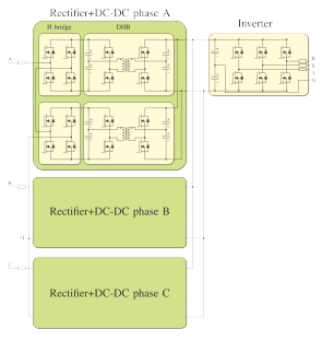 Figure 1: SST topology.
A three-stage SST is considered in this paper [7]. Its topology is shown in Figure 1. The three stages are: a rectification stage, where a three-phase high voltage (HV) AC grid voltage is converted to a DC signal, a DC-DC converter stage (multiple stages in parallel) that provides isolation and performs the level adaptation, and finally, an inverter stage that converts the DC signal into a three-phase low voltage (LV) AC sinusoidal wave.
In this paper, simple models for each stage are proposed. Using these models, the required controllers are designed and their parameters are tuned to obtain a good performance in presence of sudden load changes. In order to test the performance of the proposed controllers, simulations results are introduced.
2. Proposed SST topology and model
Figure 2 shows a general diagram of the chosen topology. The SST is composed of a bidirectional multi-level HV three-phase converter, labeled Rectifier, six bidirectional isolated DC-DC converters, labeled DHB1 through DHB6, and a bidirectional LV three-phase converter with neutral, labeled Inverter. This topology has a great degree of modularity, allowing to consider the converters as decoupled systems and simplifying the design of the controllers [7].
Each converter and its simplified model is described below. Since the controllers are implemented using digital control techniques, the models are described in discrete time, assuming a sampling time Ts.
2.1 Rectifier
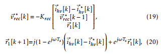
The rectifier is a three-phase AC-DC converter connected to the HV grid. As shown in Figure 2, the rectifier input port is modeled as a three-phase controlled voltage source vrec = [vreca vrecb vrecc]T , coupled to the HV grid voltage vhv = [vhva vhvb vhvc]T through an inductor with current ihv = [ihva ihvb ihvc]T . This coupling filter is modeled using complex vector notation (see Appendix). The zero order hold (zoh) discrete time model of the coupling filter results:
 The output ports of the rectifier are modeled as current sources iiX, with X = 1…6. These currents are computed through power balance. Considering that both H bridges of each phase of the rectifier are given the same reference, it can be found that their currents are equal:
 Note that in this rectifier model, the independent variables (control inputs) are the three-phase components of vrec[k].
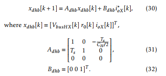
2.2 Dual Half Bridge (DHB)
Since there are six isolated DC buses in the rectifier, there are six DC-DC converters which are implemented using the DHB topology, which are modeled as current sources. The coupling between the output ports of the rectifier and the input port of each DHB is performed through a capacitor. The voltage across each of these capacitors is modeled through the difference equation:
 with X = 1…6. The DHBs themselves are controlled using a phase shift strategy. Therefore, each converter can be modeled through the algebraic equation for their average power transfer [11]:
 where m is the DHB transformer relation, Ld is the total leakage of the transformer referred to the HV side, fswdhb is the switching frequency of the DHB converter, and δX is the phase shift angle between the voltages generated at the HV and LV sides of the DHB under consideration. Dividing this power by VbusHX[k], it results
 which describes the relation between input port ioX
and the control action δX. The outputs of all the DHBs are connected in parallel, and feed the LV bus. The relation between the input signals and the output signals is obtained through power balance, as described in the following equation:
 Note that in this DHB model, the independent variable (control input) for each DHB is δX.
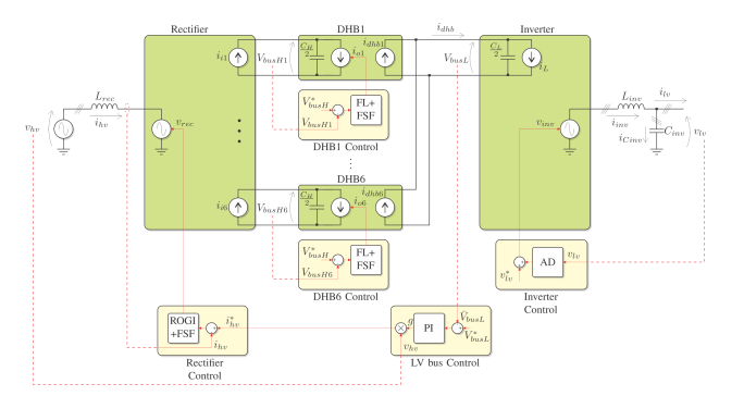 Figure 2: SST topology, model and general control scheme. Figure 2: SST topology, model and general control scheme. |
2.3 Inverter
The inverter is a three-phase DC-AC converter connected to the LV grid. The input port is modeled as a controlled current source iL, and the output port is modeled as a three-phase controlled voltage source vinv = [vinvr vinvs vinvt]T . The load voltage and current are vlv = [vlvr vlvs vlvt]T and ilv = [ilvr ilvs ilvt]T , respectively.
The coupling between the output ports of the DHBs and the input port of the inverter is performed through a capacitor. The voltage across this capacitor is modeled through the difference equation:
 The coupling between the load and the output port of the inverter is performed by an LC filter. Since each leg of the inverter is controlled as a single phase converter, the zoh discretization of this filter is given for each phase of the inverter. This is denoted with subscript Y, which can be equal to r, s or t:
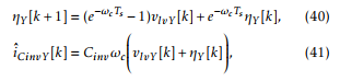
 where xinvY [k] = [iinvY [k] vlvY [k]]T ,
 As in the previous converters, the relation between the input signals and the output signals is obtained through power balance, as described in the following equation:
![]() where the • operator denotes scalar product. Note that in this inverter model, the independent variables (control inputs) are the three-phase components of vinv[k].
where the • operator denotes scalar product. Note that in this inverter model, the independent variables (control inputs) are the three-phase components of vinv[k].
3. Converter controller description
Figure 2 shows the simplified block diagrams of the proposed controllers for each converter. In this figure, dashed lines represent measured signals, and solid lines in the controllers represent control signals. In what follows, each individual controller is described.
3.1 Rectifier control
This controller is tasked to make the HV grid current ihv to copy the current reference ihv∗ . This is achieved through a full state feedback (FSF) control with the addition of a reduced order generalized integrator (ROGI) [12]. The ROGI is added to achieve zero steady state tracking error, since the current reference is a grid frequency positive sequence three-phase signal. Considering a one sample time processing delay, typical in digital implementations, complex vector notation, and space vector modulation (SVM), the control action is
 where max and min functions are computed between the abc components of v]. Also,vmc
 with Krec a 1×3 complex gain vector, and ~r1[k] represents the state of a ROGI tuned at fundamental grid angular frequency ω. As described in [12], gain vector Krec can be found using the linear quadratic regulator method, or by pole placement using Ackerman’s formula, and the matrix description of the system:
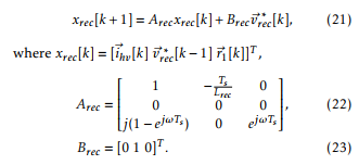
The reference ihv∗ is the output of the LV bus controller, and it is related to the instantaneous HV grid voltage throughwhere xrecT ,
![]() where g is a scalar variable signal. Therefore, depending on the sign of g and assuming vhv sinusoidal with no harmonic distortion, the rectifier will source or sink a three-phase sinusoidal current to the HV grid, with unity power factor. In this paper the closed loop poles are chosen to achieve a settling time of 4.5[ms].
where g is a scalar variable signal. Therefore, depending on the sign of g and assuming vhv sinusoidal with no harmonic distortion, the rectifier will source or sink a three-phase sinusoidal current to the HV grid, with unity power factor. In this paper the closed loop poles are chosen to achieve a settling time of 4.5[ms].
3.2 DHB control
The objective of the DHBs is to transfer the pulsating power of each of the H bridges of the rectifier to the LV bus, where the resulting power is non-pulsating. To achieve this objective, the controller of each DHB is designed to keep its instantaneous voltage VbusHX at its reference level VbusH∗ (which is the same for all six DHBs). As shown by (7), the relation between current ioX and phase-shift angle δX is non-linear. In order to be able to apply linear control techniques, a feedback linearization (FL) is implemented. Then, the resulting linear system is controlled through FSF.
Considering a one sample time processing delay, the control action is
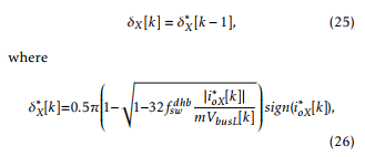 is obtained from (7) and it is the FL equation for the system. Assuming that VbusL[k] ‘ VbusL[k − 1] (slow varying signal), it can be numerically verified that for a given value of ioX∗ [k − 1], evaluating (26) at k − 1, and replacing the result in (25) and (7) yields ioX[k] ‘ ioX∗ [k − 1]. Therefore, the linearized system is modeled by (5) and
![]() Adding a discrete time backward Euler integrator to achieve zero steady state error, the control action for each DHB is computed as follows:
Adding a discrete time backward Euler integrator to achieve zero steady state error, the control action for each DHB is computed as follows:
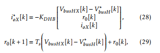 where Kdhb is a 1×3 gain vector, and r0[k] represents the state of the discrete integrator. Once (28) is computed, the phase shift angle δX∗ is obtained through (26) and applied to the converter.
Gain vector Kdhb can be found using the linear quadratic regulator method, or by pole placement using Ackerman’s formula, and the matrix description of the linearized system:
 This scheme makes each DHB source power to the LV bus if its HV bus voltage is higher than VbusH∗ , or sink power from the LV bus if its HV bus voltage is lower than VbusH∗ . In this paper the closed loop poles are chosen to achieve a settling time of 1[ms].
3.3 LV bus control
This controller is tasked to keep the mean value of the LV bus voltage (V¯busL in Figure 2) at the reference level VbusL∗ . In order to do so, signal VbusL is filtered (filter not shown in the figure) and then a proportional integral (PI) controller is used. The output of this controller is the variable gain g. This gain is used to properly scale the measured HV grid voltage, and generate the current reference for the rectifier, defined in (24). For this reason, the dynamics of the rectifier control loop and the LV bus control loop must be decoupled. This is achieved by making the bus control loop significantly slower than the rectifier and DHB control loops.
The LV bus voltage is modeled by (9). Since there is no controlled current source directly connected to the LV bus, the design of the controller assumes that idhb is the control action. Once the control action idhb is computed, gain g is obtained through power balance:
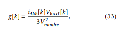 where Vnomhv is the nominal rms value of the HV grid voltage. As stated at the beginning of this section, this controller is slow. Therefore, both the processing delay and the dynamics of the filter used to obtain V¯busL can be ignored without significant error. Considering this, and adding a discrete time backward Euler integrator to achieve zero steady state error, the control action is computed as follows:
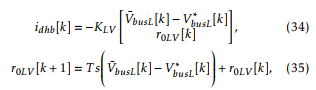 where KLV is a 1×2 gain vector, and r0LV [k] represents the state of the discrete integrator. Once (34) is computed, gain g is computed through (33), and used to generate the HV grid current reference ihv∗ through (24).
Gain vector KLV can be found using the linear quadratic regulator method, or by pole placement using Ackerman’s formula, and the matrix description of the system:
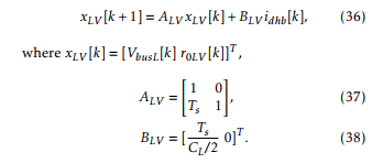
In this paper the closed loop poles are chosen to achieve a settling time of 100[ms].CL/2
3.4 Inverter control
This controller implements the active damping (AD) of the output LC filter resonance. The implementation of the AD requires to measure the current through Cinv. To avoid this measurement, an estimator through high pass filter derivation is used. This estimator only requires the measurement of vlv, and only slightly increases the settling time of the control loop. The LV grid voltage reference vlv∗ is added to the control action of the AD. This voltage reference is a three-phase balanced sinusoidal signal, which can be generated internally, or can be obtained through a synchronization algorithm in synchronism with the HV grid voltage.
Since each leg of the inverter is controlled independently, there are three equal controllers. In what follows, they are described with subscript Y = r, s or t. Considering a one sample processing time, the control action for the active damping strategy is vinvY [k] = vinvY∗ [k − 1], where
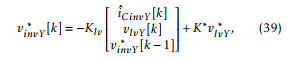 where Klv is a 1×3 gain vector, K∗ is a gain, and iˆCinvY [k] is the estimated capacitor current, obtained from the zoh discretization of a high pass filter:
with ωc the cut off frequency of the high pass filter, and ηY the state of the filter.
Gain vector Klv is obtained by pole placement to damp the LC filter resonance using Ackerman’s formula, and the matrix description of the system: xlv[k +1] 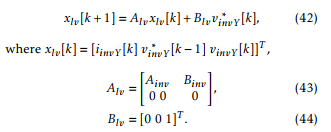
Finally, gain K∗ is included to compensate the magnitude of the LV grid voltage reference, and is obtained evaluating:
 where ACLlv = Alv − BlvKlv, I is the 3×3 identity matrix and Clv = [0 1 0]. Note that the controllers for each phase use the same gain vector Klv and gain K∗. In this paper the closed loop poles are chosen for optimal damping (ζ = 0.707). This results in a settling time of approximately 2[ms].
4. Parameter selection criteria
This section gives criteria for choosing the values of the different parameters of each converter.
4.1 Rectifier coupling inductance Lrec
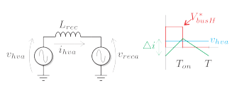 Figure 3: Rectifier phase a and switching interval variables.
The value of Lrec is chosen to obtain a desired current ripple 4i when injecting zero current to the HV grid. Due to the 5-level structure of the rectifier and the use of unipolar modulation, the effective switching frequency applied to Lrec is 4fswrec [1]. Also, this multilevel structure ensures that the voltage difference applied to Lrec will never be larger than VbusH∗ (assuming all the HV buses are kept at that level).
Taking phase a as a reference, Figure 3 shows one switching interval. The current variation in this interval is
Since zero current injection is assumed, in this interval
![]() where d = Ton/T . Therefore, replacing this in (47),
where d = Ton/T . Therefore, replacing this in (47),
 where T = 1/(4fswrec) was used. The maximum 4i occurs for d = 0.5, therefore for this condition, from (49),
![]() From Table 1, choosing the peak current ripple√ 4i/2 =
From Table 1, choosing the peak current ripple√ 4i/2 =
0.1( 2Inomhv), the inductance results Lrec = 190[mH]. From an additional analysis not included in this paper, considering commercially available cores, Lrec = 200[mH] is chosen.
4.2 DHB transformer leakage inductance Ld
From (6), assuming VbusHX[k] = VbusH∗ and VbusL[k] =
VbusL/m the maximum power transfer occurs for δX[k] = π/2 and results
 Under nominal operation conditions, each DHB will have to transfer a mean power P¯dhb = Snom/6. Taking a safety margin of PdhbMAX = 2P¯dhb to catch any transients, and replacing this in (51), the leakage inductance results
 Using the necessary parameters from Table 1 to evaluate (52), it results Ld = 8.44[mH]. From an additional analysis not included in this paper, designing Ld considering commercially available cores, it results Ld = 8.8[mH] .
4.3 HV bus capacitor CH
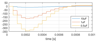 Figure 4: 4VbusH [V] for a 10% HV grid voltage dip for different values of CH.
During the event of dips or swells in the HV grid voltage vhv, there will be a transient behavior in each of the HV buses. This can lead to unacceptable under/over voltages in VbusHX. The HV buses voltage variations during these transients are determined by the value of CH, the settling time of each DHB control loop, and the magnitude of the dips or swells. Since the evaluation of these transients involves the DHB control loop, the process is iterative. For a given value of CH, gain Kdhb must be computed. Then, the performance is evaluated through a simple simulation applying the desired dip or swell magnitude. Finally, the process is repeated until the desired performance is attained.
The evaluation is performed considering a step change in the magnitude of vhv. In the following, the worst case scenario for VbusH1 is analyzed, which is similar for the remaining buses.
The maximum instantaneous power variation in phase a occurs when the rectifier is sinking nominal current, and at the instantaneous peak of vhva[k] its magnitude changes 4vhv volts. From (1), assuming that previous to the step v~hv ‘ v~rec, the magnitude of the change in the HV grid current is
![]() From (2), assuming that previous to the step VbusH1 =
From (2), assuming that previous to the step VbusH1 =
VbusH1 = VbusH∗ , the variation in current ii1 is
![]() where (53) was used for the last equality. Now the effect of 4vhv in VbusH1, defined as 4VbusH, is evaluated simulating the closed loop response of the linearized DHB (30)-(32):
where (53) was used for the last equality. Now the effect of 4vhv in VbusH1, defined as 4VbusH, is evaluated simulating the closed loop response of the linearized DHB (30)-(32):
 where Bidhbi = [CHTs/2 0 0]T and Acldhb = Adhb − BdhbKdhb. Figure 4 shows simulation results for this system for CH = 10 [µF], 1[µF] and 0.5[µF] when a 10% dip is simulated (4vhv = −0.1Vnomhv) for the DHB control designed with a settling time of 1[ms]. From the results CH = 1 [µF] is chosen, since it results in a 2.5% voltage variation.
4.4 LV bus capacitor CL
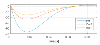 Figure 5: 4VbusL [V] for a nominal load sudden connection and different values of CL.
The value of capacitor CL is chosen so that in the event of a sudden nominal load connection, the LV bus voltage does not go below the minimum value required for normal operation. The minimum LV bus voltage required for operation is
![]() where the value is obtained from Table 1. Therefore, a conservative design criterion is to keep VbusL > 700V when a nominal load is connected. This is equivalent to obtain a LV bus voltage variation 4VbusL < 100V .
where the value is obtained from Table 1. Therefore, a conservative design criterion is to keep VbusL > 700V when a nominal load is connected. This is equivalent to obtain a LV bus voltage variation 4VbusL < 100V .
To evaluate the LV bus voltage variation for different values of CL, gain vector KLV is computed for each given value, and then a simulation is performed. From (36)-(38), the following system is simulated:
![]() where ACLLV = ALV − BLV KLV , BclLV = −BLV and 4iL = Snom/VbusL∗ . Figure 5 shows simulation results for this system for CL = 5 [mF], 10[mF] and 15[mF] when a nominal load is suddenly connected and the LV bus voltage control loop is designed with a settling time of 100[ms]. From the results all capacitor values meet the requirements, however CL = 10 [mF] is chosen because of reduced ripple under unbalanced load conditions.
where ACLLV = ALV − BLV KLV , BclLV = −BLV and 4iL = Snom/VbusL∗ . Figure 5 shows simulation results for this system for CL = 5 [mF], 10[mF] and 15[mF] when a nominal load is suddenly connected and the LV bus voltage control loop is designed with a settling time of 100[ms]. From the results all capacitor values meet the requirements, however CL = 10 [mF] is chosen because of reduced ripple under unbalanced load conditions.
4.5 Inverter filter LinvCinv
The typical output impedance of a standard transformer is 2%-5% of its base impedance. Therefore, Linv is chosen so that its impedance at angular frequency ω is 2% of the base impedance:
![]() On the other hand, capacitor Cinv limits the bandwidth of the output. Here, to obtain a fast transient response, the cut-off angular frequency of the output filter is chosen
On the other hand, capacitor Cinv limits the bandwidth of the output. Here, to obtain a fast transient response, the cut-off angular frequency of the output filter is chosen
![]() Since the resonance frequency of the filter is approximately equal to the cut-off frequency, 1
Since the resonance frequency of the filter is approximately equal to the cut-off frequency, 1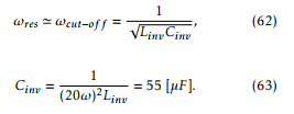
5. Operation analysis of the control system and simulation results(20ω)
This section presents simulation results of the proposed SST when a load is suddenly connected and disconnected. Additionally, results for sudden nonlinear load connection are included. The results are obtained using the switching models of all converters. The system parameter summary is shown in Table 1.
Table 1: System parameter summary
| RECTIFIER AND LV BUS | ||
| Param. | Value | Description |
| Snom | 20[kVA] | SST nominal power |
| Vnomhv | 7621[Vrms] | HV nom. phase voltage |
| Inomhv | 0.875[Arms] | HV nom. phase current |
| ∗ | 800[V] | |
| fswrec | 8[kHz] | Switching frequency |
| DHB | ||
| CH | 1[µF] | HV bus capacitor |
| CLdhb | 56[µF] | LV DHB capacitor |
| Ld | 8.8[mH] | DHB leakage ind. |
| ∗ | 6000[V] | |
| fswdhb | 20[kHz] | Switching frequency |
| INVERTER | ||
| Linv | 461.2[µH] | LC filter ind. |
| Cinv | 55[µF] | LC filter cap. |
| Vnomlv | 220[Vrms] | LV phase voltage |
| fswinv | 20[kHz] | Switching frequency |
The controllers were designed so that the rectifier control loop has a settling time of 4.5[ms], the DHB control loop has a settling time of 1[ms], and the LV bus voltage control loop has a settling time of 100[ms]. The settling time of the inverter AD loop is defined by the cutoff frequency of its LC output filter plus the estimation of the current through Cinv. This settling time results approximately 2[ms].
5.1 Sudden load connection
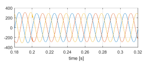 Figure 6: vlv [V] sudden load connection.
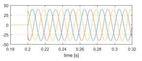 Figure 7: ilv [A] sudden load connection.
 Figure 8: VbusL [V] sudden load connection.
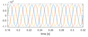 Figure 9: vhv [V] sudden load connection.
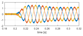 Figure 10: ihv [A] sudden load connection.
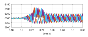 Figure 11: VbusH1−VbusH6 [V] sudden load connection.
The simulation results shown in Figures 6-11 start at t = 0.18[s] with the SST in steady state, with no load connected on the LV side. This means that the HV and LV buses start at their reference voltage levels and that a balanced three-phase sinusoidal voltage vlv is generated without taking significant current ihv from the HV grid.
At t = 0.2[s] a resistive nominal load is connected at the inverter output. The following sequence of events occurs (refer to Figure 2 for the definition of the variables):
- Figures 6 and 7 show vlv and ilv, respectively. As expected, when the load is connected vlv has a short transient.
- Through power balance, current source iL takes current from capacitor CL, reducing voltage VbusL as shown in Figure 8. As can be seen, its settling time is approximately 100[ms], as designed.
- The LV bus voltage control loop detects the reduction of V¯busL, increasing in turn the value of g, resulting in g > As a result, current reference magnitude increases.
- Commanded by its current controller, the rectifier sinks active power from the grid, with unity power factor. Figures 9 and 10 show vhv and ihv, respectively. Here the settling time of the current is tied to the settling time of g, defined by the LV bus control loop.
- Through power balance, the current source outputs of the rectifier charges capacitors CH of the HV buses, increasing their voltage levels. The voltages of the HV buses is shown in Figure 11.
- The control loop of each DHB detects the increase in their respective HV bus voltage VbusHX. As a result, it commands each DHB to sink current ioX in order to decrease the instantaneous value VbusHX to its reference value VbusH∗ once again. This results in the short transient increase in the mean value of voltages VbusHX seen in Figure 11. Through power balance, each output current idhbX sources current to the LV bus, charging CL to VbusL∗ again, as shown in Figure 8.
By the end of this sequence, in steady state, the system is delivering power to the load and taking current with unity power factor from the HV grid.
5.2 Sudden load disconnection
 Figure 12: vlv [V] sudden load disconnection.
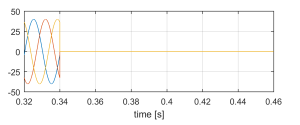 Figure 13: ilv [A] sudden load disconnection.
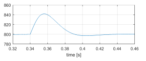 Figure 14: VbusL [V] sudden load disconnection.
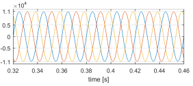 Figure 15: vhv [V] sudden load disconnection.
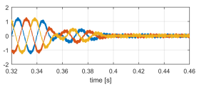 Figure 16: ihv [A] sudden load disconnection.
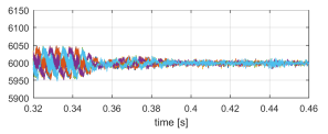 Figure 17: VbusH1−VbusH6 [V] sudden load disconnection.
Starting from the previous condition, if the load is now disconnected, the following sequence of events will occur:
- Figures 12 and 13 show vlv and ilv, respectively. As expected, when the load is disconnected vlv has a short transient.
- Through power balance, current source iL stops sinking current from capacitor CL, which charges because the DHBs are still transferring power from the HV grid. This is seen in Figure14.
- LV bus voltage control loop detects the voltage increase in V¯busL, decreasing in turn the value of g, resulting in g < As a result, current reference ihv∗ magnitude decreases.
- Commanded by its current controller, the rectifier goes from sinking to supplying active power to the grid, with unity power factor. Figures 15 and 16 show vhv and ihv, respectively.
- Through power balance, the current source outputs of the rectifier discharge capacitors CH of the HV buses, decreasing their voltage levels, as seen in Figure 17.
- The control loop of each DHB detects the decrease in their respective HV bus voltage VbusHX. As a result, it commands each DHB to source current ioX in order to increase the instantaneous value VbusHX to its reference value VbusH∗ once again. This results in the short transient decrease in the mean value of voltages VbusHX seen in Figure 17. Through power balance, each output current idhbX sinks current from the LV bus, discharging CL to VbusL∗ again, as shown in Figure 14.
By the end of this sequence, in steady state, the system has its buses at their reference values, and the inverter generates vlv without sinking current ihv from the HV grid.
5.3 Sudden non-linear load connection
The simulation of section 5.1 is repeated for the sudden connection of a balanced non-linear load. For each phase of the inverter, the load is composed of a single phase rectifier, feeding a 1[mH] inductor in series an RC load where R and C are in parallel (with R=19.5[Ω] and C=1[µF]). The results of this simulation are shown in Figures 18-23. As can be seen in these results, the proposed topology works well under highly non-linear load conditions.
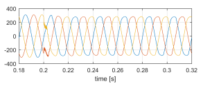 Figure 18: vlv [V] sudden non-linear load connection.
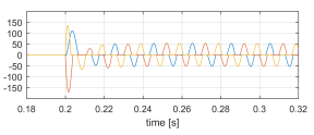 Figure 19: ilv [A] sudden non-linear load connection.
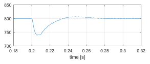 Figure 20: VbusL [V] sudden non-linear load connection.
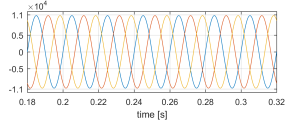 Figure 21: vhv [V] sudden non-linear load connection.
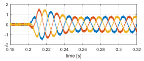 Figure 22: ihv [A] sudden non-linear load connection.
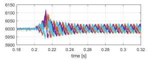 Figure 23: VbusH1−VbusH6 [V] sudden non-linear load connection.
5.4 Sudden non-linear unbalanced load connection
The simulation of the previous section is repeated, using the same non-linear load, but connecting these loads to only two of the three phases. The results of this simulation are shown in 24-29. As can be seen in these results, the proposed topology also works well for unbalanced non-linear loads.
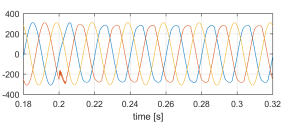 Figure 24: vlv [V] sudden non-linear unbalanced load connection.
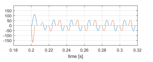 Figure 25: ilv [A] sudden non-linear unbalanced load connection.
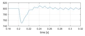 Figure 26: VbusL [V] sudden non-linear unbalanced load connection.
 Figure 27: vhv [V] sudden non-linear unbalanced load connection.
 Figure 28: ihv [A] sudden non-linear unbalanced load connection.
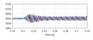 Figure 29: VbusH1 − VbusH6 [V] sudden non-linear unbalanced load connection.
6. Conclusions
In this paper a model and a control strategy for an SST topology is proposed. The analyzed SST is designed using three separate stages: a rectifier, a DCDC converter and an inverter. The proposed design approach is to model each stage using simple models. These simple models help to design and tune the controllers for each stage. The main focus of the tuning procedure is to obtain good performance to sudden load connections. Criteria to choose the main parameters of the SST are also given.
To validate the proposed method, simulation results are presented. The results show that the proposed topology and control strategies perform as expected from design conditions. Moreover, the staged design of the SST allows to decouple the HV side from the LV side in regard to load disturbances, which is an additional feature of the SST when compared to traditional transformers. Simulations were performed for both linear and non-linear loads. Moreover, a nonlinear unbalanced load was also tested, with good performance results.
Acknowledgment
The authors are grateful to CONICET, UNIVERSIDAD NACIONAL DEL SUR and AN-
PCyT for their institutional and economic support
- C. Busada, H. Chiacchiarini, S. G. Jorge, F. Mengatto, A. Oliva, J. Solsona, G. Bloch, and A. Delgadillo, “Modeling and control of a medium voltage three-phase solidstate transformer,” in 2017 11th IEEE International Conference on Compatibility, Power Electronics and Power Engineering (CPE-POWERENG), April 2017, pp. 556–561. DOI: 10.1109/CPE.2017.7915232
- J. Van der Merwe and H. d. T. Mouton, “The solidstate transformer concept: A new era in power distribution,” in AFRICON 2009, 2009. DOI: 10.1109/AFRCON. 2009.5308264
- G. T. Heydt, “The next generation of power distribution systems,” IEEE Transactions on Smart Grid, vol. 1, no. 3, pp. 225– 235, 2010. DOI: 10.1109/TSG.2010.2080328 [4] S. Falcones, X. Mao, and R. Ayyanar, “Topology comparison for solid state transformer implementation,” in IEEE PES General Meeting. IEEE, 2010, pp. 1–8. DOI: 10.1109/PES.2010.5590086
- S. Falcones, X. Mao, and R. Ayyanar, “Topology comparison for solid state transformer implementation,” in IEEE PES General Meeting. IEEE, 2010, pp. 1–8. DOI: 10.1109/PES.2010.5590086
- X. She, R. Burgos, G. Wang, F. Wang, and A. Q. Huang, “Review of solid state transformer in the distribution system: From components to field application,” in 2012 IEEE Energy Conversion Congress and Exposition (ECCE). IEEE, 2012, pp. 4077–4084. DOI: 0.1109/ECCE.2012.6342269
- X. She, A. Q. Huang, and R. Burgos, “Review of solid-state transformer technologies and their application in power distribution systems,” IEEE Journal of Emerging and Selected Topics in Power Electronics, vol. 1, no. 3, pp. 186–198, 2013. DOI: 10.1109/JESTPE.2013.2277917
- J.W. Kolar and G. Ortiz, “Solid-state-transformers: key components of future traction and smart grid systems,” in Proc. of the International Power Electronics Conference (IPEC), Hiroshima, Japan, 2014.
- F. Wang, A. Huang, X. Ni et al., “A 3.6 kv high performance solid state transformer based on 13kv sic mosfet,” in 2014 IEEE 5th International Symposium on Power Electronics for Distributed Generation Systems (PEDG). IEEE, 2014, pp. 1–8. DOI: 10.1109/PEDG.2014.6878693
- J. E. Huber and J. W. Kolar, “Volume/weight/cost comparison of a 1mva 10 kv/400 v solid-state against a conventional low-frequency distribution transformer,” in 2014 IEEE Energy Conversion Congress and Exposition (ECCE). IEEE, 2014, pp. 4545–4552. DOI: 10.1109/ECCE.2014.6954023
- Z. Yu, R. Ayyanar, and I. Husain, “A detailed analytical model of a solid state transformer,” in 2015 IEEE Energy Conversion Congress and Exposition (ECCE). IEEE, 2015, pp. 723–729. DOI: 10.1109/ECCE.2015.7309761
- H. Fan and H. Li, “High-frequency transformer isolated bidirectional dc-dc converter modules with high efficiency over wide load range for 20 kva solid-state transformer,” IEEE Transactions on Power Electronics, vol. 26, no. 12, pp. 3599– 3608, Dec 2011. DOI: 10.1109/TPEL.2011.2160652
- C. A. Busada, S. G. Jorge, A. E. Leon, and J. A. Solsona, “Current controller based on reduced order generalized integrators for distributed generation systems,” IEEE Transactions on Industrial Electronics, vol. 59, no. 7, pp. 2898–2909, July 2012. DOI: 10.1109/TIE.2011.2167892