A Switched-Capacitor Low-Pass Filter with Dynamic Switching Bias OP Amplifiers

Adv. Sci. Technol. Eng. Syst. J. 2(6), 100–106 (2017);
 DOI: 10.25046/aj020613
A switched capacitor low-pass filter employing folded-cascode CMOS OP Amps with a dynamic switching bias circuit capable of processing video signals, which enables low power consumption, and operation in wide bandwidths and low power supply voltages, is proposed. In this filter, charge transfer operations through two-phase clock pulses during the on-state period of the OP Amps and a non-charge transfer operation during their remaining off-state period are separated. Through simulations, it was shown that the low-pass filter with an OP Amp switching duty ratio of 50 % is able to operate at a 14.3 MHz high-speed dynamic switching rate, allowing processing video signals, and a dissipated power of 68 % of that observed in the static operation of the OP Amps and a full charge transfer operation without separation of a cycle period. The gain below -31 dB in the frequency response, which is suitable, was obtained at over 6 MHz within a stop-band. Especially high attenuation in 5 MHz was achieved under the optimized condition of load capacitances (4 pF) of OP Amps.
1. Introduction
The switched capacitor (SC) techniques are appropriate for realizing various filters that can be integrated in monolithic ICs (Integrated Circuits) from using the CMOS (Complementary Metal-Oxide-Semiconductor) technology. In conventional active RC filters, monolithic ICs cannot be realized from using resistors. On the contrary, the CMOS SC techniques suitable for realizing analog signal processing ICs, have promising use in video signal bandwidth circuits in particular, because these can replace resistors to switched capacitor pairs with small capacitances. It has been demonstrated that SC techniques using CMOS operational amplifiers (OP Amps) are useful for implementing analog functions such as filtering [1-5]. Although CMOS OP Amps are suitable for such filter ICs, the use of several OP Amps results in large power consumption. Especially, the power consumption of OP amplifiers in high speed operation becomes large because they have wideband properties. Therefore, the use of them is currently limited to the use in low-frequency passband of at most a few hundred kHz (that is, applications of low speed signal processing, such as analog voice signals).
Until now, several approaches have been considered to decrease the power consumptions of OP Amps, including the development of ICs that work at low power supply voltages [6]. A clocked current bias scheme for folded-cascade OP Amps suitable for achieving a wide dynamic range has typically been proposed to decrease the power consumption of the OP Amp itself [7, 8]. Because the circuit requires complicated four-phase bias-current control pulses and biasing circuits, it results in a large layout area and is not suitable for the high-speed operation. A control method using power supply switching has been proposed for audio signal processing as another approach in decreasing the power consumption of OP Amps [9]. Because large capacitors for the power supply terminals are intrinsically loaded, the switching speed is limited to a low speed of 1 MHz at most. Therefore, this type of control circuit is not suitable for application to video signal processing ICs, which are required to operate at over 10 MHz switching frequency.
Recently, the author proposed a folded-cascade CMOS OP Amp with a dynamic switching bias circuit (DSBFC OP Amp), of simple configuration, to provide low power consumption while maintaining high speed switching operation suitable for processing video signals [10]. However, low-power signal processing circuits such as wideband filters with such DSBFC OP
Amp, suitable for processing video signals, have not been developed yet.
In this paper, a configuration of SC Butterworth low-pass filter (LPF) with DSBFC OP Amps [11] as an example of application of the DSBFC OP Amp is proposed, which enables low power consumption and is suitable for achieving wide bandwidths and operation in low power supply voltages, and its availability is also evaluated for the performance of frequency response and power dissipation. Further, the effect of OP Amp load capacitances on the frequency response is evaluated. This paper is an extension of work originally presented in LASCAS 2017 [11].
2. SC Filter Theory
The discrete-time transfer function of second-order SC infinite impulse response (IIR) LPF is shown as follows using the z-transform.
![]() Here, K, bk, and z-1 represent the gain constant, the filter coefficient in a recursive loop, and the one-step delaying operation, respectively. All of operation circuits are composed of active sampled data processing circuits with a sampling circuit, switching circuits and capacitors.
Here, K, bk, and z-1 represent the gain constant, the filter coefficient in a recursive loop, and the one-step delaying operation, respectively. All of operation circuits are composed of active sampled data processing circuits with a sampling circuit, switching circuits and capacitors.
3. SC Filter Circuit Design
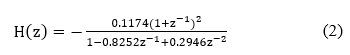
A second-order IIR LPF with the Butterworth frequency characteristic was designed because it is easy to design due to its flat gain characteristic in the passband. The Butterworth LPF is also superior to a Chebyshev filter for processing video signals owing to its ripple less characteristic within the passband. The filter order of second was selected to achieve a gain of -30 dB at a stop-band over 6 MHz. The other design condition was set as follows. That is, a sampling frequency fs=14.3 MHz, which is equal to four times as much as the NTSC color sub-carrier frequency 3.58 MHz, and a cutoff frequency fc=2 MHz, respectively, were chosen, that enable the LPF to process video signals. Under this condition, the inverted discrete-time transfer function is given by
 The circuit configuration realizing this transfer function is shown in Figure 1. In order to enable easily to determine the capacitance value of each capacitor, the coefficient of A is set to be equal to that of B. Capacitors can be basically divided into two groups. In one group (C, D, E, and G), charges are supplied to OP Amp 1. In another group (A, B, and I), charges are supplied to OP Amp 2. Even if a capacitance of each capacitor group is multiplied by constant times, the transfer function does not change. Therefore, capacitances of integral capacitors B and D are here selected as a reference capacitance in each group and each coefficient of B and D is normalized to 1. At this time, 1 as every normalized coefficient of A, B, and D is obtained because A and B are the same coefficient. In Figure 1, when the coefficients of A, B, and D are normalized to 1, other coefficients are determined as follows.
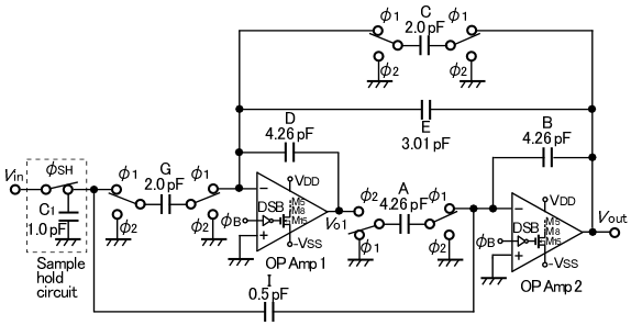 Figure 1: Configuration of the 2nd-order SC LPF with DSBFC OP Amps
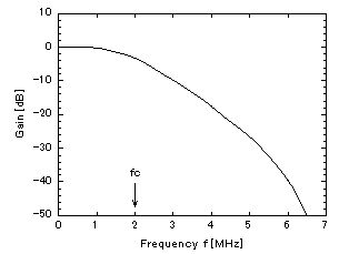 Figure 2: Theoretical frequency response of the 2nd-order SC Butterworth LPF
I=K=0.1174
G=2K+2I=0.4694
C=1+b1+b2=0.4694
E=1-b2=0.7054
Here, b1=-0.8252 and b2=0.2946. When the smallest coefficient of I=0.1174 is replaced as a reference capacitance of 0.5 pF, each capacitance in the SC IIR LPF IC is set in proportion to the above coefficients as shown in Figure 1. Because its input signal is desirable to be maintained by a sample/hold circuit for stabilizing, this sampling circuit is also applied in the SC LPF. At this time, the transfer function is multiplied by the following zero-order hold function due to a sample-hold effect.
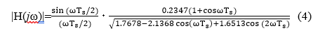
![]() Here, Ts represents a cycle period of sampling and switching pulses. Therefore, when the function of (2) is replaced using z= , the magnitude of the transfer function of the second-order SC LPF considering the sample-hold effect is given by (4).
Here, Ts represents a cycle period of sampling and switching pulses. Therefore, when the function of (2) is replaced using z= , the magnitude of the transfer function of the second-order SC LPF considering the sample-hold effect is given by (4).
 The theoretical frequency response including the sample-hold effect is shown in Figure 2. The SC LPF configuration was designed referencing a SC biquad circuit with integrators in the
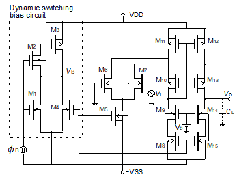 Figure 3: Configuration of the DSBFC OP Amp
reference [12]. It consists of a sample-hold circuit with a holding capacitor C1 and a CMOS sampling switch controlled by φSH, CMOS switches φ1, φ2, capacitors A, B, C, D, E, G, and I, and two FC CMOS OP Amps with the DSB circuit (DSBFC OP Amps). A configuration of the DSBFC OP Amp enabling low power consumption, which is different from conventional ordinary OP Amps [10], is shown in Figure 3. With respect to the DSBFC OP Amps, the same CMOS channel width / length as that in the DSBFC OP Amp shown in the reference [10] was employed. The sampling switch was designed to a channel width / channel length W/L=35/2.5 (μm/μm) for each of p-MOSFET and n-MOSFET. The holding capacitor C1 has a small capacitance of 1 pF. CMOS switches with a W/L=25/2.5 (μm/μm) are turned on and off by non-overlapping two-phase clock pulses φ1 and φ2, swinging from -2.5 V to 2.5 V. These sampling and CMOS switches are designed to have a balanced structure with each equal length and width of p-channel and n-channel MOSFETs (component of these CMOS switches) to delete a feed-through phenomenon, which is caused by gate clock pulses due to a capacitive coupling between gate and CMOS-switch output terminals. Major CMOS process parameters are given as a gate insulating film thickness tox=50 nm, an n-MOSFET threshold voltage VTn=0.6V, and a p-MOSFET threshold voltage VTp=-0.6 V.
The operation principle of this LPF is simply described in the following. The output signal Vo1 of OP Amp 1 is obtained as an additional output of an integrated signal of Vin using a negative integrator (D, G SC circuit, and OP Amp 1), an integrated signal of Vout using a negative integrator (D, C SC circuit, and OP Amp 1), and a signal multiplied Vout by E/D. The output signal Vout is an additional output of an integrated signal of Vo1 using a positive integrator (A SC circuit, B, and OP Amp 2), and a signal multiplied Vin by I/B. Vout is basically fed back to an input of OP Amp 1 like this. Vin is also integrated twice and added after being decreased by an appropriate capacitance ratio. Due to these integration using positive / negative integrators, addition and feedback operations, the function of LPF is achieved.
The operation waveforms of the SC LPF are shown in Figure 4. In this SC LPF, charge transfer operations through the clock
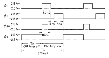 Figure 4: Operation waveforms of the 2nd-order SC LPF
pulses φ1 and φ2 are achieved during the on-state period of the DSBFC OP Amps. The off-state period TB (the remaining period of the one cycle period Ts) is separately provided to realize low power dissipation for the SC LPF. An input signal is sampled during the sampling phase of φSH (10 ns) and the first period of clock phase φ1, while its corresponding charge is stored on the holding capacitor C1, and is transferred to an output terminal Vout, charging all capacitors. The voltage at the off transition of φSH is kept on C1 during the remaining period of clock phase φ1. During subsequent clock phase φ2, each charge of two capacitors C and G is discharged and each charge of remaining capacitors is redistributed. These charge transfer operations are achieved during the on-state period of the OP Amps. During this period, the OP Amps turn on by setting a bias voltage of VB at an appropriate level enabling M3 and M4 to operate in the saturation region, and operate normally as operational amplifiers. φB is set to low just before φ1 changes to high.
Subsequently, φB becomes 2.5 V at the off-state transition of the OP Amps, at the same time φ2 is switched to off. During this off period TB, the OP Amps turn off by setting VB at nearly -2.5 V enabling M1 to operate in a low impedance and M3 in a high impedance. Therefore, during this off period, the OP Amps do not dissipate at all. When TB is relatively long as compared to the one cycle period Ts, the power dissipation is expected to become lower than that observed in ordinary static operation for the SC LPF using conventional OP Amps. If half GB (Gain Bandwidth product) OP Amps for the SC LPF are used in the static operation (without DSB operation), rise and fall times to stable states of filter output signals will increase to much larger than twofold, because slowly changing transition occurs at the end of transition. Therefore, an expected proper filter performance will not be able to be obtained when such OP Amps are used.
4. Simulation Results
The performance of the SC LPF was investigated by simulation using the SPICE (Simulation Program with Integrated Circuit Emphasis) program package. Operation waveforms for an input signal of 1 MHz with an amplitude of 0.3 V and an output load capacitance of 1 pF are shown in Figure 5. For the passband frequency signal, the same level output signal as the input one was obtained. The frequency response of the SC LPF is shown in Figure 6 (a) in the dynamic switching operation of the DSBFC OP Amps and (b) in the on-state (static operation) of the DSBFC
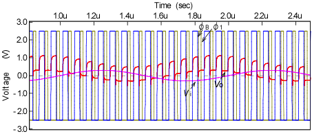 Figure 5: Simulation waveforms for the 2nd-order SC Butterworth LPF. Input signal=0.3 V0–P, Input signal frequency fin=1 MHz
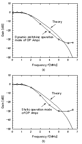 Figure 6: Frequency response of the 2nd-order SC Butterworth LPF. (a) Dynamic switching operation mode of the DSBFC OP Amps, TB=35 ns, (b) Static operation mode of the DSBFC OP Amps, φB=-2.5 V
OP Amps at φB= -2.5 V. The uncertainty of gain characteristics in simulation is nearly 1 dB at the frequency of 6.5 MHz. The frequency responses in case of both modes are almost the same for the in-phase state, in which the maximum output signal is
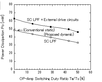 Figure 7: Power dissipation vs. OP Amp switching duty ratio in the 2nd-order SC LPF. fin=1 MHz. A constant pulse width of 15 ns for φ1 and φ2 was used
obtained depending on a phase between the input signal and the sampling pulse. The response was near the theoretical one from 100 kHz up to near 5 MHz, in the high frequency range over 6 MHz, it deteriorated due to a sampling phase effect. The gain below -33 dB was obtained at over 6 MHz within a stop-band. This was superior to that in the static operation. Therefore, it is thought that there is almost no gain deterioration caused by employing the DSB operation of the OP Amps. Though the stop-band gain in the second order LPF is not low enough as shown above, it is expected that the roll-off in the frequency response will become steeper by increasing the filter order, and so the stop-band gain will greatly decrease. Therefore, the achievement of a wide stop-band with a high attenuation will become possible.
Power dissipation vs. OP-Amp switching duty ratio with φ1=φ2=15 ns is shown in Figure 7. The power dissipation of the SC LPF itself excluding that of external drive circuits for φSH, φ1, φ2, and φB decreased in proportion to the off period TB of the Op Amps as expected. In the operation mode of TB=35 ns (=50 % switching duty ratio) and φ1=φ2=15 ns, the power dissipation of the SC LPF (32.9 mW) was decreased to 68 % as compared to that in the static operation of the OP Amps (48.5 mW). In the full charge transfer operation without separation of the one cycle period Ts (φ1=φ2=30 ns), the power dissipation of the LPF was 48.5 mW, the same as that in the static operation of the OP Amps with the above separated charge transfer mode. Most of the power dissipation of the SC LPF corresponds to total power consumption dissipated in the OP Amps themselves. The power consumption of the external drive circuits was nearly 13~14 mW. Thus, even when two DSBFC OP Amps are applied to the SC LPF, the dynamic operation of the DSBFC OP Amps enabling low power dissipation as compared to their static operation is also useful for reducing the power dissipation of SC LPF. When the SC LPF is operated at a lower dynamic switching rate, because it enables TB/Ts to become larger than 50 %, the power dissipation of the SC LPF is expected to decrease in proportion to TB still more. This means that the SC LPF with high-speed DSB operation OP Amps is advantageous compared to the SC LPF using static operation OP Amps with a lower GB.
Table 1: Performance comparison of SC LPFs with CMOS technology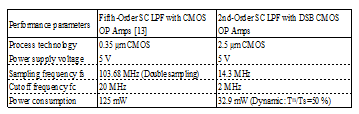
When the filter order is increased, a SC LPF with DSB OP Amps uses OP Amps of the number of filter order. Therefore, the power dissipation of this SC LPF is expected to increase in proportion to its filter order. The power dissipation for the reported fifth-order SC LPF employing conventional CMOS OP Amps with a 5-V power supply and a 0.35-μm CMOS technology was 125 mW as shown in the performance comparison of Table 1 [13]. If a fifth-order SC LPF using the DSB OP Amps with the sampling frequency fs=14.3 MHz is achieved, its power dissipation will be estimated to be 82.3 mW. Considering that the power consumption of OP Amps parts in each LPF is dominant, a comparison between these values is possible. Obviously, the estimated power dissipation of a revised version of the proposed SC LPF with DSB OP Amps is much less than that of the above conventional fifth-order SC LPF.
5. Effect of Load Capacitances
Because the DSBFC OP Amp switches dynamically, its output becomes a quasi-floating state during the off-state period. In the off-state period of the OP Amp, though MOSFETs M5, M8, and M15 turn to the off-state completely, MOSFETs M11 and M12 become the on-state strongly because over the threshold voltage between each gate and source is applied. At this time MOSFETs M6, M7, M9, M10, M13, and M14 become the on-state weakly. The output terminal Vo of the OP Amp is set to a voltage depending on the load capacitance through the capacitive coupling between the drain and the gate of the MOSFET M13. Therefore, when a large output swing in Vo occurs at the off-state transition, there is a fear that the output voltage during the subsequent on-state period of the OP Amp suffers the influence of this transition. So, a dynamic offset voltage Voff (the difference of the on-state and the off-state output voltages of the OP Amp) at the off-state transition of the OP Amp vs. load capacitance CL was tested and is shown in Figure 8. Obviously, the dynamic offset voltage depends on the load capacitance and decreases as its load capacitance becomes large because CL compared to the drain-gate capacitance in M13 becomes large. The change of Voff against CL of the SC LPF resembles to that of the OP Amp (Figure 9). This means that Voff of the SC LPF is mainly determined by the OP Amp’s dynamic off-state transition. Gain vs. OP Amp load capacitance (of two OP Amps) for the SC LPF is shown in Figure 10. In this case, the phase between the input signal Vin and the sampling signal φSH was fixed to a constant value in each input signal to avoid the sampling phase effect. The gain became the minimum at a load capacitance of nearly 4~5 pF for the input signal frequency of 5 MHz. The reason is explained in the following. In small load capacitances, Voff is not only large, but also its variation is not negligible depending on the on-state output voltage. This phenomenon causes the on-state output voltage’s difficulty to
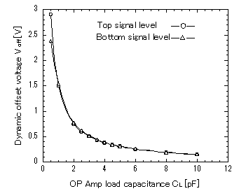 Figure 8: Dynamic offset voltage vs. load capacitance in the DSBFC OP Amp. Input signal=0.00085 V0–P, Input signal frequency fin=0.5 MHz, Cutoff frequency fc at CL of 1 pF =4.13 MHz
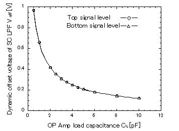 Figure 9: Dynamic offset voltage vs. OP Amp load capacitance in the SC LPF. Input signal Vin=0.3 V0–P, Input signal frequency fin=5 MHz
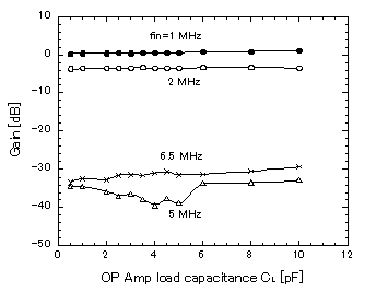 Figure 10: Gain vs. OP Amp load capacitance in the SC LPF
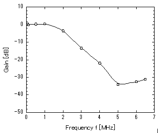 Figure 11: Frequency response of the SC LPF. OP Amp load capacitance
CL=4 pF
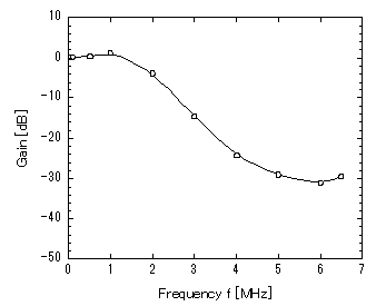 Figure 12: Frequency response of the SC LPF. OP Amp load capacitance
CL=10 pF
reach its steady state completely within the short time period of 15 ns (in φ1 or φ2), while permitting its output voltage to change slightly (bringing about the SC LPF gain’s deterioration). In large load capacitances, it becomes also hard to reach its steady state within 15 ns (causing the gain’s deterioration) due to OP Amp’s bandwidth deterioration although Voff and its variation are very insignificant. However, at an optimum capacitance of nearly 4 pF, its gain deterioration becomes slight due to small offset transition with slight offset voltage variation and fast transition to the steady state. For other input signals of low frequencies (1, 2 MHz), the variation effect of Voff is negligible due to its large output signal (the change of gains is hardly seen) although its variation depending on the output signal voltage is relatively large in small load capacitances. Of course, since Voff and its variation for these low frequencies are negligibly small in large load capacitances, the change of gains with CL is dominated by only OP Amp’s bandwidth deterioration. For the 6.5 MHz input signal, though the gain is basically determined due to the sampling phase effect, it is slightly changing with CL due to OP Amp’s bandwidth deterioration.
Under the optimized load capacitance of 4 pF, the frequency characteristic of gain for the SC LPF was tested. As shown in Figure 11, its high frequency gain of near 5 MHz improved drastically (over 4.3 dB compared to the gain in the load capacitance CL of 1 pF). Though its gain increased slightly (up to -31 dB) in 6.5 MHz, the amount of its gain increase is slight. On the contrary, when CL is increased to 10 pF larger than the optimized value, the frequency response of the SC LPF deteriorated in high frequencies over 5 MHz (Figure 12). Thus we can see that the SC LPF gain characteristics can be improved by the optimization of load capacitances of DSB OP Amps. Typical characteristics are listed in Table 2.
Table 2: Typical characteristics of SC LPF with DSB OP Amps (VDD=VSS=2.5 V)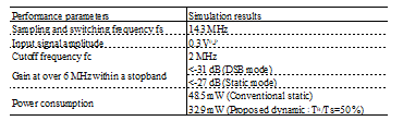
Conclusions
A switched capacitor low-pass filter employing folded- cascode CMOS OP Amps with a dynamic switching bias circuit capable of processing video signals, which enables low power consumption, operation in wide bandwidths and low power supply voltages, was proposed and its performance was evaluated. In this SC LPF, charge transfer operations through two-phase clock pulses during the on-state period of the OP Amps and non-charge transfer operation during the remaining off-state period of the OP Amps were separated. Through SPICE simulations, it was shown that the SC LPF is able to operate at a 14.3 MHz high-speed dynamic switching rate, allowing processing video signals, and a dissipated power of 68% of that observed in the static operation of the OP Amps and the full charge transfer mode without separation of the one cycle period. The power consumption in the SC LPF body except for the external drive circuits was that of OP Amps. When rearranging these results, it became clear that a lower-dissipated-power SC LPF employing DSB folded-cascode CMOS OP Amps compared to conventional SC LPFs with static operation OP Amps can be realized. The gain below -31 dB in the frequency response, which is suitable, was also obtained at over 6 MHz within a stop-band.Especiallyhighattenuationin5MHzwasachievedundertheoptimizedconditionofloadcapacitances(4pF)ofOPAmps.
Thus, the dynamic charge transfer operation during the on-state period of the OP Amps and non-charge transfer operation during their off-state period is useful for high speed operation, and reducing the power dissipation of the SC LPF. This circuit should be useful for the realization of low-power wide-band signal processing ICs including over one of multi-order low-pass, high-pass and band-pass filters. The DSB circuit achieving such operation can be applied to not only folded-cascode but telescopic, two-stage, and rail-to-rail OP Amps.
- Gregorian and W. E. Nicholson, “CMOS Switched-Capacitor Filters for a PCM Voice CODEC,” IEEE J. Solid-State Circuits, SC-14(6), 970-980, Dec. 1979.
- Dessoulavy, A. Knob, F. Krummenacher, and E. A. Vittoz, “A Synchronous Switched Capacitor Filter,” IEEE J. Solid-State Circuits, SC-15(3), 301-305, June 1980.
- Iwata, H. Kikuchi, K. Uchimura, A. Morino, and M. Nakajima, ”A Single-Chip Codec with Switched-Capacitor Filters,” IEEE J. Solid-State Circuits, SC-16(4), 315-321, Aug. 1981.
- -T. Wu, Y.-H. Chang, and K.-L. Chang, “1.2 V CMOS Switched-Capacitor Circuits,” in 1996 IEEE International Solid-State Circuits Conference Digest of Technical Papers-42nd ISSCC, 388-389, 479.
- Chatterjee, Y. Tsividis, and P. Kinget, “Ultra-Low Voltage Analog Integrated Circuits,” IEICE Trans. Electronics, E89-C(6), 673-680, June 2006.
- Kun, W. Di, and L. Zhangfa, “A High-Performance Folded Cascode Amplifier,” in 2011 International Conference on Computer and Automation Engineering-ICCAE 2011, IPCSIT, 44, 41-44, 2012.
- B. Kasha, W. L. Lee, and A. Thomsen, “A 16-mW, 120-dB Linear Switched-Capacitor Delta-Sigma Modulator with Dynamic Biasing,” IEEE J. Solid-State Circuits, 34(7), 921-926, July 1999.
- L. Chen, Y. S. Lee, and J. S. Chiang, “Low Power Sigma Delta Modulator with Dynamic Biasing for Audio Applications,” in 50th Midwest Symposium on Circuits and Systems 2007-MWSCAS 2007, 159-162.
- Wang, J. Xu, and X. Wu, “A Low Power Audio Delta-Sigma Modulator with Opamp-Shared and Opamp-Switched Techniques,” in Proceedings of the International MultiConference of Engineers and Computer Scientists 2010-IMECS 2010, 1296-1300.
- Wakaumi, “A Folded-Cascode OP Amplifier with a Dynamic Switching Bias Circuit,” Engineering Letters, 23(2), 92-97, June 2015.
- Wakaumi, “A Switched-Capacitor Filter with Dynamic Switching Bias OP Amplifiers,” in 8th Latin American Symposium on Circuits and Systems-LASCAS 2017, 33-36, Feb. 2017.
- Takebe, J. Iwata, N. Takahashi, and H. Kunieda, Switched Capacitor Circuit, Tokyo: Gendai Kohgaku-Sha, Apr. 2005.
- -K. Moon, “CMOS High-Frequency Switched-Capacitor Filters for Telecommunication Applications,” IEEE J. Solid-State Circuits, 35(2), 212-220, Feb. 2000.