Selective Electron Beam Melting Manufacturing of Electrically Small Antennas

Adv. Sci. Technol. Eng. Syst. J. 2(6), 70–75 (2017);
 DOI: 10.25046/aj020609
Real estate pressures in modern electronics have resulted in the need for electrically small antennas, which have subsequently garnered interest amongst researchers and industry alike. These antennas are characterized by their largest dimensions translating to a fraction of the operating wavelength; such a diminutive size comes at the expense of reduced gain and efficiency, and a worse overall match to a corresponding power source. In order to compensate for this deterioration in performance, antenna designers must turn towards increasingly complex and voluminous geometries, well beyond the capabilities of traditional manufacturing techniques. We present voluminous metal antennas, based on a novel inverted-F design, and fabricated using the emergent selective electron beam melting manufacturing technique, a type of powder bed fusion process. As predicted by small antenna theory, simulation results presented show in increase in the antenna’s efficiency as it is voluminously expanded into the third dimension. Measurement results illustrate that key trends observed from simulations are upheld; however, further understanding of the electromagnetic properties of raw materials, in particular how these change during the printing process, is needed. Nevertheless, this type of additive manufacturing technique is suitable for rapid prototyping of novel and complex antenna geometries, and is a promising avenue for further research and maturation.
1. Introduction
With the continued trend of miniaturization in the design and manufacture of modern, ‘smart’ electronics, antenna designers are challenged with delivering compact, low-cost, and easy to fabricate antennas, often operating at wavelengths many times their largest dimension. A further key requirement is that these antennas are made efficient, so as to prolong battery life. This paper is an extension of work originally presented in the 2017 International Workshop on Antenna Technology in Athens, Greece [1]. The discourse on additively manufactured (AM) voluminous antennas is expanded to provide an overview of electrically small antennas (ESA) in literature fabricated using novel techniques, the three-dimensional (3D) powder bed fusion (PBF) printing process, the antenna design process, as well as the implications of simulated and measured results on practical antenna design.
Formally, an antenna is classed as electrically small if the product of the wavenumber, k (= 2π/λ), and the radius of an imaginary sphere circumscribing the maximum dimension of the antenna, a, is less than or equal to 0.5; note that the parameter ka is unit-less [2-4]. It is widely accepted that as the electrical size of an antenna is reduced, its performance (in terms of gain, efficiency, and bandwidth) deteriorates. Generally, the radiation resistance decreases, while the reactive component of its impedance increases, leading to a poor match with the feed line or network. As such, there is a compromise between miniaturization and performance; small antenna theory dictates that a favourable compromise is reached when the antenna fully occupies a volume defined by the radius a [2-8]. Consequently, there is tremendous potential in the successful manufacture of novel, 3D antenna geometries – hitherto too complex to fabricate with traditional processes – using emergent technologies such as holographic photolithography, 3D printing, direct-write printing, direct transfer patterning, thermal transfer printing, and aerosol jet printing [9-18].
PBF-AM is a particularly attractive technology, as it has the capability to print with metallic raw materials, simplifying the production line compared to some of the other additive techniques cited above. Techniques such as stereolithography and aerosol jet printing entail first printing a plastic or ceramic component, and then subsequently coating it with a layer of metal. Direct-write techniques are serial in nature, and thus slower and unsuitable for mass manufacture. Patterning techniques are suspect to wear and tear of the mechanical stamping parts. All of these processes require a substrate for subsequent metal patterning, whereas no such limitation applies to PBF-AM.
Simulated results for radiation efficiency are presented for a type of planar inverted-F antenna (PIFA), introduced in [19], as it is voluminously extended into the 3rd dimension. The results are validated with three PBF-AM fabricated antennas: flat, part-spherical (~66% fill-factor), and full-spherical (~100% fill-factor), using the Wheeler cap method [20-22]. Radiation pattern measurements are provided for two full-spherical prototypes to compare the effects of fabrication tolerances. The main aims of this research are to present measurement results on pioneering 3D antennas fabricated using AM, and to assess the viability of this emergent technique, in its current state, as a possible fabrication method for inherently 3D antennas. In particular, two popular PBF-AM techniques – which make use of a laser and an electron beam as the heat source, respectively – are compared and the relative strengths and weaknesses assessed.
2. Background on Additive Manufacture
Additive manufacture, also known as 3D printing, is the umbrella term given to a range of processes where raw materials are formatively shaped, layer by layer, to form a desired object or part [23, 24]. A generic illustration of a PBF printer is provided in Figure 1; the technology can be used on a wide range of plastics and metals, and has the obvious advantages of speed, reduced waste, and greatly simplified production lines. In particular, PBF-AM is an attractive technology for antenna manufacture as it is one the few subcategories of 3D printing which can handle metallic raw materials. Compared to other AM techniques, PBF is also advantageous with respect to operating costs, albeit at the expense of higher power consumption and lower build volumes. Two common heat sources used in PBF are lasers and electron beams, leading to the respective processes termed as selective laser melting (SLM) and selective electron beam melting (SEBM).
For this research, the laser based Renishaw AM250 and the electron beam based Arcam A2 printers were used. The difference in heat source leads to some inherent differences in the printing process. In an SLM printer, the chamber is typically filled with inert gas in order to minimize oxidation and degradation of the powdered material. A pressurized vacuum environment is necessary in the SEBM printer, otherwise the bombarded electrons would interact with atoms in the gas and thus get deflected. The electron beam can also be moved a lot faster than the laser, leading to shorter build times. Energy delivered by the electron beam is, however, more diffuse than a laser, leading to a greater area affected by the heat. Consequently, the minimum feature size, resolution, and surface-finish of the SEBM process are typically worse off compared to SLM.
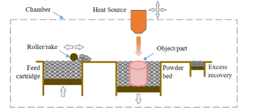 Figure 1. Illustration of generic PBF-AM printer.
In both processes, the powder in the build platform is maintained at an elevated temperature, typically just below its melting point and/or glass transition temperature; the build platform itself may be heated with the help of resistive heaters. For SLM, this elevated temperature allows for lowering the power rating of the laser, and prevents faults that might arise due to non-uniform thermal expansion and contraction. In the SEBM process, the powder is further heated to slightly sinter the particles prior to bombardment from the electron beam. This is done primarily to increase conductivity throughout the powder, to allow the negatively charged electrons to swiftly affect the desired object region. This eliminates the need for any sacrificial support structures under overhanging features, which are sometimes required in SLM printers.
3. Experimental Procedure
3.1. Antenna Design
Figure 2 shows the front profile view of the PIFA variant, based on the original design reported in [19]; the metallization is approximately 0.7 mm thick, resting on a hollow substrate with the same wall thickness, with the entire back side metallized to form the ‘ground plane’. The centrally placed digitated structure contributes to a lowering of the resonance frequency of the antenna through additional capacitance and inductance. In fact, there are two current paths on this structure, contributing to orthogonally polarized modes, which may be tuned closer together with the relative positioning of the feed point and shorting pin, thereby increasing the effective bandwidth of the antenna. However, this was not a focus of the current research, as uncertainties in material properties and manufacturing tolerances meant that the focus was shifted purely to comparative efficiency measurements. Note than an extensive parametric study on antenna design and performance is presented in the reference [19], and is applicable to the voluminous antennas presented here.
This template is used for three variations of antennas with different voluminous expansions: flat, part-spherical, and full-spherical, as shown in Figure 3. For each antenna, the maximum radius, and parameter a, is 15.0 mm. Simulated results for the resonance frequency and efficiency as a function of the parameter h (as described in Figure 3) are provided in Figure 4 and Figure 5, respectively. It can be seen from Figure 5 that the 2nd resonance varies more as a function of the voluminous expansion, h, as compared to the 1st resonance, with the general trend that the respective resonance frequencies reduce as h increases, since the currents have a longer effective length on a more curved surface. The corresponding radiation efficiency at resonance also exhibits a general trend, where the efficiency increases as h is increased and the antenna occupies more and more of the Chu sphere. For the 2nd resonance, the radiation efficiency of the flat antenna is 14%, increasing to 68% for the full-spherical antenna. Establishing an overall trend for this particular antenna geometry, at the dimensions specified, a unit (1 mm) change in height h results in an increase in radiation efficiency of 1.6 percentage points. Thus, the PIFA based antennas may be made more efficient, subsequently delivering power savings in appliances, at the cost of increased cross-sectional profile.
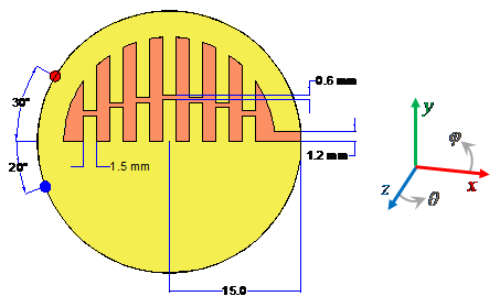 Figure 2. Schematic of top metallization for flat profile. Red dot is feed point; blue dot is shorting point. Back is fully metallicized.
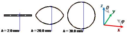 Figure 3. Cross-sectional view of CAD models simulated in CST Microwave Studio ®, for progressively greater voluminous expansion.
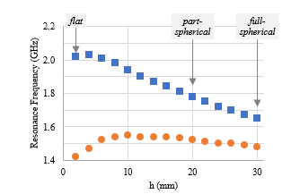 Figure 4. Simulated resonance frequency of (orange) 1st and (blue) 2nd resonances as a function of h. Fabricated antennas are annotated.
3.2. Fabricated Prototypes
The SLM process was trialed first, on a Renishaw AM250 printer, in order to take advantage of its superior surface finish. However, the process is much less capable of manufacturing overhanging features such as the centrally populated digits. Where this limitation is usually overcome with the use of sacrificial support structures analogous to scaffoldings used in building construction, the removal of such structures proved too damaging to the delicate digits.
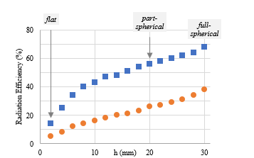 Figure 5. Simulated radiation efficiency of (orange) 1st and (blue) 2nd resonances as a function of h. Fabricated antennas are annotated.
A photograph of an antenna part fabricated with SLM is shown in Figure 6a, with the support structures partly removed. To alleviate this limitation, the antenna parts were subsequently fabricated using the SEBM based Arcam A2 printer. There is no need for support structures in this technique, as the metallic powder is pre-sintered before being melted by the electron beam. However, the poorer surface finish is evident from the photograph in Figure 6b. This is due to the use of coarser powder layers with the SEBM process (40-105 µm compared to 15-45 µm for the laser process), and the comparatively larger area affected at any one time by the electron beam compared to a heating laser.
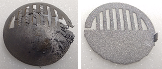 Figure 6. Photographs of metallic antenna parts fabricated using (a) SLM, and (b) SEBM
In total, three variations of the same antenna design were fabricated: flat, part-spherical, and full-spherical; two of these are pictured in Figure 7. The antenna radiator and ground plane were fabricated separately using a Titanium alloy, Ti-6Al-4V (σ ≈ 105 Sm-1). Hollow plastic substrates fabricated from the plastic nylon12 were used to provide support. Copper tape was subsequently used to short the top metallization to the ground plane, and to provide contact pads for soldering Sub Miniature version A (SMA) connectors for interfacing to a power source. For this batch of antennas, a total of 18 parts were printed in just under two and a half hours; the build specifications for these antennas using the Arcam A2 printer are as follows:
- the printer was run under a vacuum of about 0001 mbar, with a slight amount of helium inserted into the chamber to help dissipate excess charge induced into the powder bed by the electron beam,
- a stainless-steel base plate was heated to 730 °C by the electron beam before any powder was deposited,
- for each layer of powder deposited (50 µm thick), the beam was first defocused and scanned across the layer at a high speed (30 ms-1) with 2.3 kW power, for around 15 seconds, to sinter the powder,
- each part area was subsequently melted using a focused beam with a back and forth raster pattern at a speed of around 0.35 ms-1 with 300 W power,
thereafter, successive powder layers were deposited and the previous sintering and melting steps repeated until the antenna parts were fully realized.
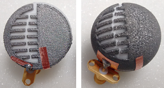 Figure 7. Photographs of SEBM PBF-AM fabricated antenna prototypes, shown assembled; (a) flat, and (b) full-spherical.
4. Results and Discussion
Return loss measurements for the flat, part-spherical, and full-spherical antennas were conducted using the Agilent E5071B vector network analyser. Radiation efficiency (for 20 MHz bandwidth) was subsequently computed using the using the constant-loss-resistor Wheeler cap method described in [22]. Note that efficiency results were computed for the second resonance only as this is the dominant resonance from measurements, and that repeat measurements per prototype exhibit an error margin of ±10 %.
The corresponding simulations were carried out using CST Microwave Studio ®, using the frequency-domain solver. The titanium alloy was approximated using copper (Cu) metal properties in the CST material library, with reduced conductivity, σ. A notable limitation of using PBF-AM for manufacturing antenna parts is the relative lack of knowledge regarding the electromagnetic properties of the raw materials; this is in fact an active area of current research in the AM community [23, 25-27]. As such, these were iteratively refined in simulations. However, the general trends in performance observed can be interpreted as a validation of small antenna theory, as well as the usefulness of AM techniques in the swift prototyping of non-conventional antenna geometries.
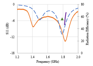 Figure 8. S11 results for PBF-AM part-spherical prototype; (orange) measured, (blue) simulated. Radiation efficiency at respective resonance frequencies, for the 2nd resonance; (purple) measured, (green) simulated.
Figure 9-11 compare the measured and simulated S11 parameter for the flat, part-spherical and two full-spherical prototypes, respectively. Note that S11 is the scattering parameter as obtained from a vector network analyser and is relatable to other reflectivity figures of merit such as return loss and reflection coefficient, and is typically presented in decibels (dB) [28]. Simulated efficiency at resonance and measured efficiency for 20 MHz bandwidth about the resonance frequency are also displayed. Despite differences in the absolute values for S11 and radiation efficiency, it can be seen that general trends are corroborated, as expected from small antenna theory. Computed radiation efficiency values for the 2nd resonances exhibit an increase as the voluminous expansion of the PIFA is increased.
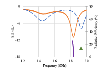 Figure 9. S11 results for PBF-AM flat prototype; (orange) measured, (blue) simulated. Radiation efficiency at respective resonance frequencies, for the 2nd resonance; (purple) measured, (green) simulated.
For the two full-spherical prototypes, despite the S11 curves following a similar curve, there is a difference of 50 MHz in the 2nd resonance. The mean radiation efficiency at resonance for the two prototypes is 68 %, with a discrepancy of 16 percentage points. Again, these differences are primarily due to inherent manufacturing differences in the antenna parts, as well as manual tolerances for the application of solder and copper tape contact pads. The differences in absolute values between simulations and measurements can be attributed to a number of factors, including unknown changes in material properties during the printing process, the presence of solder and copper tape for electrical contact to the SMA connector, as well as the rough surface finish on the antenna parts.
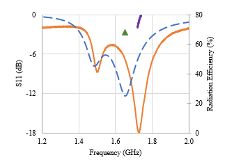 Figure 10. S11 results for PBF-AM full-spherical prototype-A; (orange) measured, (blue) simulated. Radiation efficiency at respective resonance frequencies, for the 2nd resonance; (purple) measured, (green) simulated.
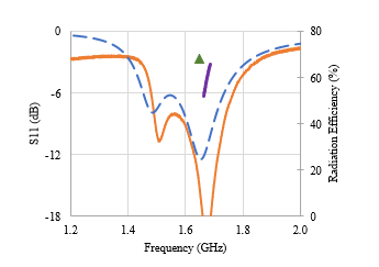 Figure 11. S11 results for PBF-AM full-spherical prototype-B; (orange) measured, (blue) simulated. Radiation efficiency at respective resonance frequencies, for the 2nd resonance; (purple) measured, (green) simulated.
Lastly, the realized gain for the full-spherical antenna prototypes was measured in an anechoic chamber, with an Agilent E5071C vector network analyser. Due to the particular feed location for this antenna, partial power gains were measured with respect to vertical and horizontal polarizations, and the gain transfer method [29] used subsequently to compute the total realized gain. Fig 6 and Fig. 7 plot the results for azimuth and elevation planes, respectively, measured at 1.7 GHz; the absolute gain is presented here in units of decibels-over-isotropic (dBi). It can be seen from these plots that simulation and measurement results largely agree, and are expectedly low directivity; there are some artifacts due to the setup (antenna holder) in the azimuth plane towards the rear of the antenna. Key results for the 2nd resonance of each antenna are summarized in Table 1.
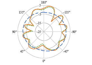 Figure 12. Realized gain (dBi) for the full-spherical ESA at 1.7 GHz; (orange) measured – sample A, (green) measured – sample B, (blue) simulated; azimuth (z-x) plane. Combined absolute gain (φ and θ components).
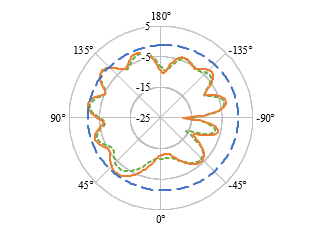 Figure 13. Realized gain (dBi) for the full-spherical ESA at 1.7 GHz; (orange) measured – sample A, (green) measured – sample B, (blue) simulated; elevation (x-y) plane. Combined absolute gain (φ and θ components).
Table 1. Simulated and measured resonant frequency and radiation efficiency at 2nd resonance for PBF-AM fabricated antennas. Measured and simulated gain at 1.7 GHz is provided for the two full-spherical antennas.
|
5. Conclusions and Future Work
This paper presents work done on voluminous, additive manufactured antennas based on a novel PIFA design. Measured results for return loss, radiation efficiency, and radiation pattern are presented for four prototypes manufactured using the SEBM based Arcam A2 printer. The metallization was realized from a Titanium alloy, Ti-6Al-4V, and hollow support substrates printed from nylon12. Copper tape was subsequently used to solder SMA connectors, and to short the top metallization to the respective antenna ground planes.
Radiation efficiency results corroborate the trends expected from simulations and small antenna theory. The mean radiation efficiency of 68% for the full-spherical antennas represents an improvement of 57 percentage points over their flat counterpart. The next stage of this project is to obtain an improved understanding of the material properties of metallic powders used in the printing process, as it has been demonstrated that the PBF-AM technique is viable for quick prototyping of complex and voluminous antenna geometries too difficult to realize using traditional fabrication techniques. Finally, the use of laser as the heat source would greatly improve the surface finish, but comes at the cost of limitations on the complexity of antenna geometry
- S. Mufti, A. Tennant, L. Seed, C. J. Smith, “Efficiency measurements of additive manufactured electrically small antennas” in 2017 International Workshop on Antenna Technology: Small Antennas, Innovative Structures, and Applications, Athens, Greece, 2017. https://doi.org/10.1109/IWAT.2017.7915397
- S. R. Best, “Small and fractal antennas” in Modern Antenna Handbook, C. A. Balanis, Ed. John Wiley & Sons, 2008, pp. 475–528.
- J. L. Volakis, C. C. Chen, K. Fujimoto, Small Antennas: Miniaturization Techniques and Applications, McGraw-Hill, 2010.
- K. Fujimoto, H. Morishita, Modern Small Antennas, Cambridge University Press, 2014.
- L. J. Chu, “Physical limitations of omni-directional antennas” J. Appl. Phys., 19(12), 1163–1175, 1948. https://doi.org/10.1063/1.1715038
- J. S. McLean, “A re-examination of the fundamental limits on the radiation Q of electrically small antennas” IEEE T. Antenn. Propag., 44(5), 672–676, 1996. https://doi.org/10.1109/8.496253
- A. D. Yaghjian, S. R. Best, “Impedance, bandwidth, and Q of antennas” IEEE T. Antenn. Propag., 53(4), 1298–1324, 2005. https://doi.org/10.1109/TAP.2005.844443
- C. Pfeiffer, “Fundamental Efficiency Limits for Small Metallic Antennas” IEEE T. Antenn. Propag., 65(4), 1642–1650, 2017. https://doi.org/10.1109/TAP.2017.2670532
- A. Maiden, “Lithography in three dimensions using computer-generated holograms,” Ph.D. Thesis, Durham University, 2005.
- D. E. Anagnostou, A. A. Gheethan, A. K. Amert, K. W. Whites, “A direct-write printed antenna on paper-based organic substrate for flexible displays and WLAN applications” J. Disp. Technol., 6(11), 558–564, 2010. https://doi.org/10.1109/JDT.2010.2045474
- J. J. Adams et al., “Conformal printing of electrically small antennas on three-dimensional surfaces” Adv. Mater., 23(11), 1335–1340, 2011. https://doi.org/10.1002/adma.201003734
- J. Hoerber, J. Glasschroeder, M. Pfeffer, J. Schilp, M. Zaeh, J. Franke, “Approaches for additive manufacturing of 3D electronic applications” Proc. CIRP, 17, 806–811, 2014. https://doi.org/10.1016/j.procir.2014.01.090
- J. J. Toriz-Garcia et al., “Fabrication of a 3D electrically small antenna using holographic photolithography” J. Micromech. Microeng., 23(5), no. 055010, 2013. https://doi.org/10.1088/0960-1317/23/5/055010
- C. Pfeiffer, X. Xu, S. R. Forrest, A. Grbic, “Direct transfer patterning of electrically small antennas onto three-dimensionally contoured substrates” Adv. Mater., 24(9), 1166–1170, 2012. https://doi.org/10.1002/adma.201104290
- M. Kgwadi, C. J. Vourch, D. J. Harrison, T. D. Drysdale, “On-demand printing of antennas for TV white-space communications” in 2014 Loughborough Antennas and Propagation Conference, Loughborough, UK, 2014. https://doi.org/10.1109/LAPC.2014.6996448
- I. T. Nassar, T. M. Weller, “An electrically-small, 3-D cube antenna fabricated with additive manufacturing” in 2013 IEEE Radio and Wireless Symposium, Austin, USA, 2013. https://doi.org/10.1109/RWS.2013.6486708
- O. S. Kim, “3D printing electrically small spherical antennas” in 2013 IEEE Antennas and Propagation Society International Symposium, Orlando, USA, 2013. https://doi.org/10.1109/APS.2013.6711047
- H. Yuxiao, C. Oakley, P. Chahal, J. Albrecht, J. Papapolymerou, “Aerosol Jet printed 24 GHz end-fire quasi-Yagi-Uda antenna on a 3-D printed cavity substrate” in 2017 International Workshop on Antenna Technology: Small Antennas, Innovative Structures, and Applications, Athens, Greece, 2017. https://doi.org/10.1109/IWAT.2017.7915352
- S. Mufti, A. Tennant, L. Seed, “Electrically small modified planar inverted-F antenna” in 9th European Conference on Antennas and Propagation, Lisbon, Portugal, 2015.
- E. Newman, P. Bohley, C. Walter, “Two methods for the measurement of antenna efficiency” IEEE T. Antenn. Propag., 23(4), 457–461, 1975. https://doi.org/10.1109/TAP.1975.1141114
- D. M. Pozar, B. Kaufman, “Comparison of three methods for the measurement of printed antenna efficiency” IEEE T. Antenn. Propag., vol. 36(1), 136–139, 1988. https://doi.org/10.1109/8.1084
- D. Agahi, W. Domino, “Efficiency measurements of portable-handset antennas using the Wheeler cap” Applied Microwave and Wireless, 36(1), 34–42, 2000.
- I. Gibson, D. W. Rosen, B. Stucker, Additive Manufacturing Technologies: Rapid Prototyping to Direct Digital Manufacturing, Springer, 2010.
- F. Calignano et al. “Overview on Additive Manufacturing Technologies” P. IEEE, 105(4), 593–612, 2017. https://doi.org/10.1109/JPROC.2016.2625098
- Y. Huang, M. C. Leu, J. Mazumder, A. Donmez, “Additive manufacturing: current state, future potential, gaps and needs, and recommendations” J. Manuf. Sci. E-T ASME, 137(1), no. 014001, 2015. https://doi.org/10.1115/1.4028725
- J. A. Slotwinski, E. J. Garboczi, “Metrology needs for metal additive manufacturing powders” JOM, 67(3), 538–543, 2015. https://doi.org/10.1007/s11837-014-1290-7
- S. K. Everton, M. Hirsch, P. Stravroulakis, R. K. Leach, A. T. Clare, “Review of in-situ process monitoring and in-situ metrology for metal additive manufacturing” Mater. Design, 95, 431–445, 2016. https://doi.org/10.1016/j.matdes.2016.01.099
- D. M. Pozar, Microwave Engineering, 4th ed, John Wiley & Sons, 2011.
- C. A. Balanis, Antenna Theory: Analysis and Design, 4th ed, John Wiley & Sons, 2016.