IGS: The Novel Fast IC Power Ground Network Optimization Flow Based on Improved Gauss-Seidel Method

Adv. Sci. Technol. Eng. Syst. J. 2(3), 711–721 (2017);
 DOI: 10.25046/aj020391
With silicon technology further scaling, the switching activities together with GHz operation frequency greatly affects the power integrity by generating large IR-drop noises. Excessive IR-drop causes functional failures such as timing failure, abnormal reset and SRAM flipping. The PGN needs to be optimized to reduce IR-drop. The traditional EDA optimization routine repeats the steps such as generating layout, extracting parameter and simulation, which greatly increases the cost of integrated circuit design. This paper proposes a novel fast optimization flow optimizing the PGN based on the improved Gauss-Seidel method (IGS), which calculates the accurate IR-drop distribution according to the initial voltage distribution and the 3-D parasitic resistance distribution of PGN. The proposed optimization flow compares the calculated IR-drop distribution with the IR-drop distribution constraints, and changes the parameters of power straps until the performance of PGN meets the requirement of constraints without full chip simulation, which reduces the time cost of PGN optimization. This paper also provides the comparison between the IGS-based optimization flow and traditional EDA optimization routine. The difference of IR-drop distributions calculated by the proposed optimization flow and traditional EDA optimization routine is less than 4.7%. And the PGN optimization time has been reduced by 96.2% on average for ITC99 benchmark s9234, s13207, s35932 and b19. According to the results and analysis, the IGS-based optimization flow is reliable to improve the performance of PGNs.
1. Introduction
For advanced technologies like 28nm and below, billions of CMOS gates are integrated into a modern SOCs. As a result, the density of power ground network (PGN) has been greatly increased, which causes extra IR-drop. Due to the parasitic resistance and inductance of PGN, as well as the high current consumption, IR-drop can reach multiple hundreds millivolts, which becomes a significant challenge for IC design and test [1]. Excessive IR-drop causes functional failures such as timing failure, abnormal reset, and SRAM flipping. Hence, it is necessary to optimize the PGN and reduce IR-drop. The details of PGN optimization routine, which improves its perforeters, and checking whether the performance of PGN meets the IR-drop constraints.
The traditional optimization routine of PGN is based on EDA tools such as Synopsys IC CompilerTM and Cadence EDITM, which uses full chip simulation to calculate the IR-drop distribution. However, when the parameters of PGN are changed, the traditional EDA optimization routine repeats the steps such as generating layout, extracting parameter and simulation, which greatly increases the cost of integrated circuit design. Therefore, it is difficult to calculate the IR-drop distribution for the PGN in a short time. Also, EDA tools only understand 1-D IR-drop constraints, which is the maximum allowable IR-drop value. For example, when the IR-drop constraint is a 2-D IR-drop distributions, EDA tools cannot understand the constraint and determine whether the calculated IR-drop distribution meets the requirement of the constraint. So the traditional optimization routine cannot provide efficient and high quality PGN optimization results. Therefore, the optimization flow with ability efficiently calculating IR-drop distribution and comparing the performance of PGN with complex IR-drop constraints is of great value.
1.1. Previous Work
Several types of optimization methods to reduce IRdrop have been presented in literatures. The optimization methods proposed in [2] and [3] reduce the IR-drop by adjusting power straps such as changing the place of power straps, increasing the density of power straps where current noise is high, and amplifying the power strap area. However, the excess power straps lead to serious placement and routing problem for chips. Also it is technically difficult to increase power straps in the tape-out process. [4] presents the analysis method of Graphene-Based power distribution networks. A Walking pads method is presented in [5] and [6], which reduces IR-drop by changing the position of power supply pads according to critical path. But the changed power pads lead to distribution problem. Also, the optimization methods based on TSVs have been analysed. A thermal-aware power network design method for the power pad optimization is presented in [7]. [8] and [9] present the optimization method to reduce IR-drop by modifying the parameters and position of TSVs, which highly increases the area of chips. The optimization methods presented in [10] and [11] change the size of TSVs to reduce IR-drop. However, the size of TSVs is constant in the 28nm technologies. The optimization method presented in [12] inserts compensation cells when the delay of critical path exceeds the allowed value to reduce IR-drop. All the researches mentioned above reduce IR-drop and optimize the PGN of chips finally. But there are a few disadvantages of these methods as follows.
- These methods reduce IR-drop based on other parts of integrated circuits rather than the PGN, which leads to appended problems such as clock delay and increasing area power dissipation.
- These methods ignore the effect of power straps in PGN, which have a non-negligible impact on the IR-drop. Power straps take a large area of PGN, whose width and density are adjustable.
- These methods are used to reduce IR-drop instead of optimizing PGN, so they cannot optimize the PGN according to the IR-drop constraints.
Previous work refers to the Random Walk algorithm in [13], which is widely used to calculate the voltage distribution. And the Representative Random Walk algorithm presented in [14] establishes a relatively simple conductance model according to the width and density of the real PGN, then calculates the IR-drop distribution of the model, which is efficient to estimate the IR-drop distribution. But this algorithm cannot get accurate IR-drop distribution and calculate the voltage of each node in PGN. [15] presents the multiple triple method, which costs too much computing resource due to the high integration of the PGN. The Gauss-Seidel Method is presented in [16] to calculate the IR-drop distribution using recursive calculation. But this method only calculates the IR-drop distribution of the 2-D PGN and ignores the conductance of power rails and TSVs. Thus it cannot calculate the IR-drop distribution of the real PGN accurately. An IR-drop measurement system on chips is presented in [17]. This method adds a sensor on the basic circuit to measure the power supply noise. The unit level sensor provides a accurate IR-drop distribution of power rails, which produces extra noise. Also, the method adding a fully digital on-chip distributed sensor network is presented in [18]. The extra sensor network monitors the power supply noise across the chip continuously and generates a trace for diagnosis of the noise-induced failure. These methods spend a lot of time to repeat the full chip simulation, and change the circuit configuration. And they cannot provide a accurate voltage distribution of PGN to meet the requirement of IR-drop constraints automatically. So they cannot be used in the actual PGN.
1.2. Contributions and Paper Organization
In this paper, a novel fast optimization flow based on the improved Gauss-Seidel (IGS) method is proposed. The IGS method takes the conductance of power rail and TSV into consideration compared with the GaussSeidel method presented in [16]. The proposed IGSbased optimization flow has the following advantages.
- It optimizes the PGN by adjusting the parameters of power straps.
- It uses improved Gauss-Seidel method to calculate the IR-drop distributions for different power straps without repeating the steps such as generating layout, extracting parameter and simulation.
- It calculates the voltage of each node in the PGN accurately.
- It automatically optimizes the PGN with less manual operation and full chip simulation compared with the traditional EDA optimization routine, which saves a lot of time.
- It can provide satisfactory parameters of power straps according to 2-D IR-drop constraints.
This paper is organized as follows. In Section 2, the IGS method is presented to calculate the IR-drop of the PGN. The novel fast optimization flow of the PGN is presented in Section 3. The analysis of the results is shown in Section 4. Finally, the conclusion is presented in Section 5.
2. The Improved Gauss-Seisel Method
2.1. The Gauss-Seidel Method for the 2-D Conductance Network
In this part, the Gauss-Seidel method, which calculates the IR-drop distribution for the 2-D conductance network, is presented. Figure 1 shows a representative node i and the neighboring nodes j in a 2-D conductance network. The conductance between the node i and j is defined as gi,j, and the voltage of node i is defined as Vi. The leakage current of node i is defined as Ii. According to the Kirchhoff Voltage and Current Law, the following equation is educed, in which Ni represents the gather of neighboring nodes of node i:
X P gi,j − P Ii (1)
Vi = Vj
j∈Ni j∈Ni gi,j j∈Ni gi,j
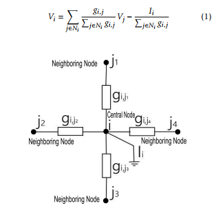 Figure 1: A representative node in the 2-D conductance Network with four neighboring nodes.
So the voltage of node i is calculated according to the leakage current of node i and the voltages of all neighboring nodes. Equation (1) is applied to all the nodes in the 2-D conductance network. A typical structure of power straps is shown in Figure 2. This model considers the network composed of power straps as the 2-D conductance network. And the intersection of power straps is regarded as a node in the calculation. The total number of nodes in the model network is N2. The conductance between the neighboring nodes (i,j) and (k,l) is defined as G(i,j) = P(k,l)∈N(i,j) |g(i,j)(k,l)|. And V(i,j) represents the gather of neighboring nodes of node (i,j). The voltage of nodes in the 2-D conductance network is calculated as:
X g(i,j)(k,l) I(i,j)
V(i,j) = V(k,l) − (2)
∈N(i,j) G(i,j) G(i,j)
(k,l)
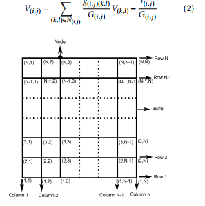 Figure 2: A typical structure of the 2-D conductance network.
The voltage distribution of the conductance network depends on the node leakage current, the volt-
ages of neighboring nodes, and the neighboring conductance. The voltage of each node in the 2-D conductance network is calculated via Equation (2). Algorithm 1 details the Gauss-Seidel method, which uses recursive computation to calculate the voltage distribution. The leakage current of each node and the conductance between neighboring nodes should be provided before calculation. The initial voltages of nodes connected to power pad is VDD, which is constant, and the initial voltages of other nodes is 0. According to the initial voltage distribution and the conductance network, the voltage distribution of the first time recursive computation is calculated via Equation (2). In this way, the new voltage of every node is presented. The second time recursive computation is based on the voltage distribution calculated by the first time recursive computation. So this method provides a accurate voltage distribution with multiple recursive computation.
Algorithm 1 The GAUSS-SEIDEL Method in the 2-D conductance network
1: Calculate related conductance value and leakage current;
2: V (0)=the initial value;
3: for each n ∈ [1,P ] do
4: for each (i,j) ∈ Q do
(n+1) X g(i,j)(k,l) (n) I(i,j)
5: V(i,j) = ∈N(i,j) G(i,j) V(k,l) − G(i,j)
(k,l)
6: end for
7: if max(abs( V (n) − V (n−1) ))< e ; then
8: break
9: end if 10: end for
Combining Algorithm 1, the first time recursive computation is finished in Line 4, and the new voltage distribution is applied to the second time recursive computation. In the process of recursive computations, the dynamic range of some parameters like the total leakage current, the total area, and the total conductance of the chip should be determined. In Algorithm 1, the parameter P on the Line 3 is the maximum times of recursive computation, which is set by users. The parameter Q represents all nodes in the power straps. The parameter e is the judgment factor to set the end of recursive computation. If the difference between adjacent computation is less than e, the recursive computation stops. The result calculated by the last time recursive computation is the output of Algorithm 1. Also, the parameter e can be used to adjust the accuracy and the time consumption of the recursive computation. With smaller judgment factor, the calculated voltage distribution is closer to the real distribution, i.e., the result is more accurate. And the results shows that the maximum value of the difference between the results calculated by the IGS-based optimization flow and traditional EDA optimization routine. Also, the smaller judgment factor leads to the increase of the iterations, which causes more time consumption of the recursive computation. However, the Gauss-Seidel Method ignores the conductance of power rails and TSVs, which influences the accuracy of voltage distribution.
2.2. The Improved Gauss-Seidel Method for the 3-D Conductance Network
The basic structure of the PGN is shown in Figure 3, which consists of three parts including power straps, TSVs, and power rails. In the PGN, the power straps connected to TSVs supplies power to TSVs. And some power rails are connected to the logic gates to feed the gates. In the actual PGN structure, the power straps can be placed in different metal layers while power rails only can be placed in one metal layer, which does not influence the analysis and calculation. This paper chooses a double layers PGN to analyse as shown in Figure 3. The leakage current only exists in power rails. The power straps and power rails with different width and density, as well as the TSVs, lead to complex conductance distribution. So the improved Gauss-Seidel method is proposed to calculate the IR-drop distribution of the 3-D PGN. The GaussSeidel method calculates the voltage distribution of the PGN, which is regarded as a 2-D conductance network. But the actual PGN has a 3-D structure consisting power straps, TSVs and power rails. Compared with the Gauss-Seidel method, the improved GaussSeidel method adopts a 3-D conductance network as the computation model to calculate the IR-drop distribution of the PGN, which is closer to the real structure of the PGN.
The first step of Algorithm 1 is calculating the conductance between neighboring nodes and the leakage current of nodes in the 2-D PGN. It is also suitable for the algorithm of the 3-D PGN. The initial voltage of power straps directly connected to the power is VDD, which is a constant in recursive computation. The initial voltage of other power straps is 0, which updates in each recursive computation. The total leakage current is measures by EDA tools, which exists in the power rails directly connected to logic gates. It is an important content to accurately calculate the equivalent conductance of metal lines in the related PGN, which depends on the volume and resistivity of metal lines. The resistivity of metal lines is provided in the standard library of chips. Figure 4 shows the equivalent transformation between the 3-D PGN and the conductance network. Each metal line is equivalent to a conductance and the metal lines network is equivalent to a conductance network. And the intersection area is regarded as a node in the equivalent transformation. The equivalent conductance networks are added to the basic conductance network to constitute the complete conductance network. And a 3-D conductance network is built in this way. There are three kind of nodes in the real PGN. The nodes formed by the horizontal and vertical power straps are defined as nodea. The nodes formed by the power straps and TSVs are defined as nodeb, The nodes formed by power rails and TSVs are defined as nodec. And the conductance between nodea is defined as ga. The conductance between nodeb is defined as gb and the conductance between nodec is defined as gc. The conductance of TSVs between nodeb and nodec is already provided as a constant.
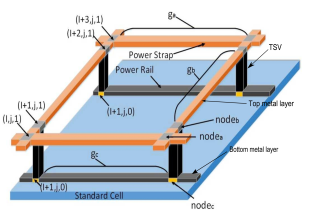 Figure 3: A two metal layers construction of the PGN consisting of power straps, TSVs and power rails.
To calculate the conductance distribution of the PGN, the total length and density of power straps should be provided. The total length of power straps is set to L and the density is set to N. The distance of neighboring nodeb is defined as lrail. The width of power straps is defined as W. And the width of power rails is defined as w. The electrical conductivity of the metal lines is defined as k. Then the conductance is calculated as:
N − 1
ga = k · · W (3)
L
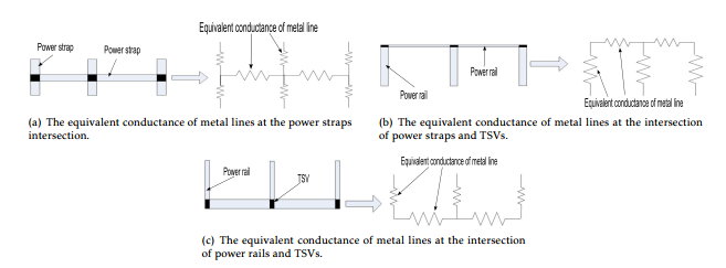 Figure 4: The equivalent transformation between the 3-D PGN and the conductance network.
gb = k · lrail · W (4)
N − 1
gc = k · · w (5)
L
The total length of chips and total leakage current, which are measured by EDA tools, are required to calculate the voltage distribution of chips. The parameters of power straps are constant except the width and density. In the PGN, which is placed in the 3D system of coordinate as shown in Figure 3, the power straps and power rails are placed in different layers, which are connected by TSVs. The nodes in the power straps are defined as (i,j,1) and the nodes in the power rails are defined as (i,j,0). The conductance between neighboring nodes (i,j,k) and (l,m,n) is defined as G(i,j,k) = P(l,m,n)∈N(i,j,k) |g(i,j,k)(l,m,n)|(k,n = 0,1). And Ni,j,k represents all the neighboring nodes of node (i,j,k). The leakage current only exists in power rails, so I(i,j,1) = 0 and I(i,j,0) , 0. The voltage of nodes in the power straps is calculated as:
X g(i,j,1)(l,m,n)
V(i,j,1) = V(l,m,n) (6)
∈N(i,j,1) G(i,j,1) (l,m,n)
And the voltage of nodes in the power rails is calculated as:
X g(i,j,0)(l,m,n) I(i,j,0)
V(i,j,0) = V(l,m,n) − (7)
∈N(i,j,0) G(i,j,0) G(i,j,0)
(l,m,n)
The voltage distribution is calculated via Equation (6) and (7). Algorithm 2 details the steps of the improved Gauss-Seidel method, which uses recursive computation to calculate the voltage distribution of the actual PGN. The conductance and leakage current of chips are provided before the algorithm.
The initial voltage of nodes connected to the power pad is VDD, which is a constant in the recursive compute process. And the initial voltage of other nodes is 0. According to the initial voltage distribution and the conductance distribution, the result of first time recursive computation is calculated via Equation (6) and (7). In this way, the new voltage distribution of the PGN is presented. Then the voltage distribution calculated by the first time recursive computation is applied to the second time recursive computation. By such analogy, the improved Gauss-Seidel method provides a accurate voltage distribution with multiple recursive computation. As well, the parameter P on the Line 3 is the maximum times of recursive computation, which is set by users. The parameter Q1 represents all nodes in the power straps, and the parameter Q2 represents all nodes in the power rails. The parameter e is a judgment factor to set the end of recursive computation in Algorithm 2. If the difference between adjacent computation is less than e, the recursive computation stops. The result of last time recursive compute is the output of Algorithm 2.Similar to the Algorithm 1, the judgement factor of Algorithm 2 determines the computational accuracy and the time consumption of the recursive computation. And the efficiency of the IGS method is inversely proportional to the value of the judgment factor. And the efficiency is proportional to the node number of the PGN as shown in Figure 4.
Algorithm 2 The Improved GAUSS-SEIDEL Method in the actual PGN
| 1: Calculate related conductance value and leakage current;
2: V (0)=the initial value; 3: for each n ∈ [1,P ] do |
|
| 4: 5: | for each (i,j,1) ∈ Q1 do
X g(i,j,1)(l,m,n) V(i,j,1) = V(l,m,n) G(i,j,1) (l,m,n)∈N(i,j,1) |
| 6: | end for |
| 7: | for each (i,j,0) ∈ Q2 do |
| 8: | X g(i,j,0)(l,m,n) I(i,j,0)
V(i,j,0) = V(l,m,n) − G(i,j,0) G(i,j,0) (l,m,n)∈N(i,j,0) |
| 9: | end for |
| 10: | if max(abs( V (n) − V (n−1) ))< e ; then |
| 11: | break |
| 12: | end if |
| 13: end for | |
3. The Novel Fast Optimization Flow Based on the Improved Gauss-Seisel Method
To optimize the PGN efficiently, a novel fast optimization flow based on the improved Gauss-Seidel method is proposed, which calculates the voltage distribution for the PGN automatically without repeating full chip simulation. This proposed optimization flow optimizes the PGN according to IR-drop constraints, which considers the conductance of power rails and TSVs. The flow diagram of this optimization flow is shown in Figure 5 and the specific steps are detailed in Algorithm 3. The proposed IGS-based optimization flow involves a three-part process of measurement, calculation and verification. The optimization process is divided into three steps. Firstly, EDA tools are used to measure the total length and leakage current of chips. Secondly, the dynamic range of power strap parameters is limited, and the IR-drop distribution of power straps is calculated by the improved Gauss-Seidel method. Finally, this proposed optimization flow understands the 2-D IR-drop distribution constraints, and compare the IR-drop distribution calculated by the IGS method and the IR-drop constraints to verify whether the performance of the PGN meets the constraints. The detailed steps of this optimization flow are described below.
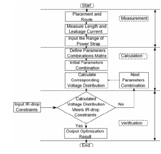 Figure 5: The flow diagram of the novel fast optimization flow diagram based on the improved Gauss-Seidel method.
3.1. Measuring the Total Length and Total Leakage Current of Chips
At the beginning of the proposed optimization flow, the total length and total leakage current of chips are provided to calculate the voltage distribution and the conductance of the PGN, which is measured by EDA tools directly. As the total leakage current is a constant when chips work at a unique frequency, EDA tools are used to place and route only once in the proposed optimization flow.
3.2. Voltage Distribution Calculation
The PGN of chips consists of three parts including power straps, power rails and TSVs as shown in Figure 3. The width and density of power rails are invariable while the width and density of power straps are adjustable. And the IR-drop can be reduced by adjusting the width and density of power straps. Before the optimization, the maximum density and minimum density of power straps are defined as Nmax and Nmin. And the maximum width and minimum width of power straps are defined as Wmax and Wmin. So the parameter group of power straps (Wα,Nβ) should satisfy the condition that Wα ∈ (Wmin,Wmax) and Nβ ∈ (Nmin,Nmax). Each parameter group represents a kind of power strap distribution of the PGN.
To traverse all possible parameter groups, the traverse gradients of the power strap width and density are defined as ∆w (∆w |Wmin − Wmax|) and ∆n (∆n |Nmin − Nmax|). The traverse gradients are determined by the actual requirements of the optimization process, which determine the optimization precision. The object of the optimization flow is to detect the PGN with satisfactory power straps, whose performance meets the requirements of the IR-drop constraints. All parameter groups are listed in a matrix as follows:
(Wmin, Nmin) (Wmin+∆w,Nmin) ··· (Wmax, Nmin)
(Wmin, Nmin+∆n) (Wmin+∆w,Nmin+∆n) ··· (Wmax, Nmin+∆n)
(Wmin, Nmin+2∆n) (Wmin+∆w,Nmin+2∆n) ··· (Wmax, Nmin+2∆n)
… … … …
(Wmin, Nmax) (Wmin+∆w,Nmax) ··· (Wmax, Nmax)
The first element (Wmin, Nmin) in matrix is the initial parameter group. Combining the parameter group with the total width and total leakage of chips measured by EDA tools, the voltage distribution is calculated using the improved Gauss-Seidel method.
3.3. Verifying Whether the Voltage Distribution Satisfies IR-drop Constraints
The IR-drop constraints provide the minimum allowable voltage of IR-drop distribution in the PGN, which is presented in Algorithm 3 as V (MIN). And the V (IGS) in Algorithm 3 indicates the minimum value of the IR-drop distribution calculated by the IGS method. If the result calculated by the IGS method meets the requirements of the IR-drop constraints, the corresponding parameter group is the result of the optimization flow, otherwise the next parameter group is applied to the IGS method to calculate the IR-drop distribution until the satisfactory IR-drop distribution is obtained.
Algorithm 3 The Novel Fast PGN Optimization Flow
1: ****** Measurement ******
2: Place and route;
3: Measure total length and total leakage current of the chip;
4: Input the Range of Power Strap and IR-drop Constraints;
5: Define parameters combinations matrix M;
6: for each (Wα,Nβ) ∈ M do
7:
8: ****** Calculation ******
9: Calculate related conductance value and current drain;
10: V (0)=the initial value;
11: for each n ∈ [1,P ] do 12: for each (i,j,1) ∈ Q1 do
X g(i,j,1)(l,m,n)
13: V(i,j,1) = V(l,m,n)
∈N(i,j,1) G(i,j,1) (l,m,n)
14: end for 15: for each (i,j,0) ∈ Q2 do
X g(i,j,0)(l,m,n)
16: V(i,j,0) = V(l,m,n) −
∈N(i,j,0) G(i,j,0) (l,m,n)
I(i,j,0)
G(i,j,0)
17: end for
18: if max(abs( V (n) − V (n−1) ))< e ; then
19: break
20: end if 21: end for
22:
23: ****** Verification ******
24: if V (IGS) − V (MIN) > 0 ; then
25: break
26: end if
27: end for
28: Output Optimization Result;
The way to compare the IR-drop distributions calculated by the IGS method and the IR-drop constraints depend on the contents of the IR-drop constraints. For example, if the IR-drop constraints only contain the maximum allowable value of IR-drop distribution, the maximum value of the IR-drop distribution calculated by the IGS method should be extracted. And if the maximum value of the calculated result is less than the maximum allowable value of IR-drop distribution, the proposed optimization flow stops and outputs the satisfactory power strap parameters of the PGN, otherwise the optimization flow continues. The proposed IGS-based optimization flow can understand the 2-D IR-drop distributions constraints such as the area ratio of different IR-drop region, and determine whether the calculated IR-drop distribution meets the requirement of the constraints. Because of the feature of the PGN, the increased width and density of power straps causes the decrease of the power strap equivalent resistances, which reduces the IR-drop finally. Therefore, when a satisfactory PGN is determined, the performance of PGNs with the wider and greater density power straps also meets the requirements of the IR-drop constraints. So the result of the proposed optimization flow is not unique. For the convenient comparison in the next section, the result of the proposed optimization flow is the PGN with the minimum parameter group, which satisfies the IRdrop constraints. But in actual conditions, all PGNs with wider and greater density power straps are acceptable.
| Benchmark | Gate Number | Leakage Current |
| s9234 | 2027 | 152mA |
| s13207 | 2573 | 76.19mA |
| s35932 | 12204 | 114.29mA |
| b19 | 67619 | 152.1mA |
Table 1: Logic Gate Number and Leakage Current of Benchmarks
4. Experimental Results
4.1. Benchmarks Under Test
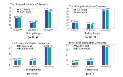
The experiments are based on the 28nm Synopsys Cell Library. In the experiment, the recursive parameter e is set to 10−7V to ensure the accuracy of the IRdrop distribution. The experiments are performed on ITC99 benchmark s9234, s13207, s35932 and b19, which are presented on ISCAS conference as the dedicated test circuits. The number of logic gates and leakage current of the selected benchmarks are shown in Table 1. And the selected benchmarks have different sizes from thousands to ten thousands to testify the wide suitability of the IGS-based optimization flow. The power panels are placed at the center, which are connected to the power straps directly. The VDD is set to 1.05V. The working frequency of the benchmarks is set to 125MHz. The IR-drop is calculated by multiplying the equivalent conductance and the leakage current of the node. And the wavelength of the 10GHz electromagnetic wave is 3cm. So the size of the chips is the small electrical size even the operation frequency reaches 10GHz. As a result, the equivalent conductance of the PGN is approximate in the 0.1 10GHz range. At different operating frequencies, the IGS-based optimization flow uses EDA tools to measure the leakage current at step one, which is determined by the operating frequency. And the measured leakage current is the input of the following steps. So the change of the operating frequency does not influence the application of the proposed optimization flow. The benchmarks are optimized according to 2-D IR-drop distribution constraints on the area ratio of different IR-drop region, and the details of the contributions are shown in Table 2. The rule of setting IR-drop distribution constraints is based on the requirements of the blocks on chips. There are a few IP cores in the SoC, which are sensitive to the slack. As a result, the IR-drop of the area with these IP cores needs to be limited strictly. So the IR-drop constraints sets a large IR-drop value of the area with sensitive
Table 2: The 2-D IR-drop Constraints on the Area Ratio of Different IR-drop region for Benchmarks
Table 3: Optimization Result and Time Overhead |
|||||||||||||||||||||||||||||||||||||||||||||||||||||||||||||||||||||||||||||||||||||
components and a small IR-drop value of other area.
The accuracy of improved Gauss-Seidel method is analyzed to validate the reliability of the proposed optimization flow. The PGNs are optimized by the IGSbased optimization flow and traditional EDA optimization routine according to the IR-drop constraints. The IR-drop distributions calculated by two methods are compared to verify the efficiency of the proposed optimization flow. The time overhead of two optimization methods is also compared.
4.2. Verifying the Accuracy of Improved Gauss-Seidel Method
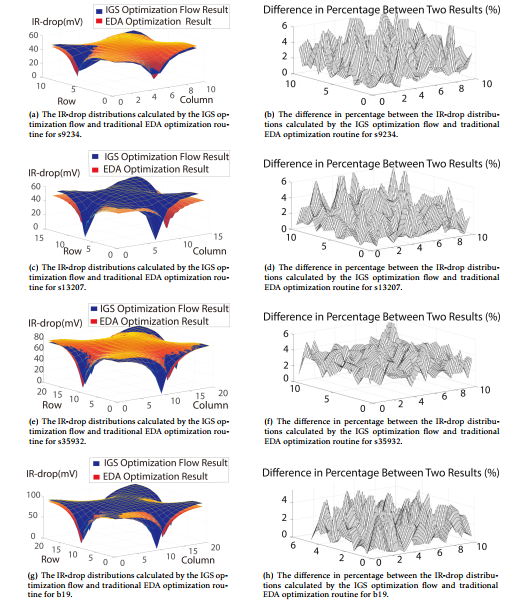
The proposed optimization flow is based on the improved Gauss-Seidel method. The IR-drop distribution, which is calculated by the improved GaussSeidel method, is a key factor to identify the performance of the PGN, so the accuracy of the improved Gauss-Seidel method determines the reliability of the proposed optimization flow. The IR-drop distributions of PGNs calculated by the improved GaussSeidel method and traditional EDA optimization routine are compared with the same IR-drop constraints to find the coherence of two methods. If the difference of two results is acceptable, the improved GaussSeidel method can be used to calculate the IR-drop distribution directly. Each benchmark is optimized by both optimization routines in the same condition. The IR-drop distributions of the PGN, which are calculated by the IGS method and traditional EDA optimization routine, are shown in Figure 6. Because of the different size of benchmarks, the IR-drop distributions are put into three dimensional coordinates to compare respectively.To highlight the gaps of the IRdrop distributions, the difference between two results is also presented in Figure 6. in Figure 6, X axis and Y axis denote the position of the nodes in power straps, and Z axis refers to the IR-drop value and the percentage of the difference as noted. The maximum value of the difference between the two results calculated by the IGS method and traditional EDA optimization routine is less than 4.7%, which proves that there is a high coherence between the two results. So the IGS method can calculate the IR-drop distribution of the PGN accurately.
Figure 7 shows the IR-drop distributions of the PGNs optimized by the IGS-based optimization flow and traditional EDA optimization routine according to the 2-D IR-drop constraints. The maximum value of the difference between two results is less than 5%. The result shows that the IGS-based optimization flow optimizes the PGN according to the IR-drop constraints on the area ratio of different IR-drop region successfully.
4.3. Analysis of Optimization Results and Time Overhead
In the optimization example, the width and density range of the power straps are set to Nmin = 10, Nmax = 30, Wmin = 0.2um, Wmax = 2um. And the variation gradient of the parameter groups is defined as ∆w = 0.02um and ∆n = 1. The 2-D IR-drop distribution constraints on the area ratio of different IR-drop region are set to prove the effectiveness of the optimization flow based on the improved Gauss-Seidel method. The optimized PGNs of the proposed optimization flow are compared with traditional EDA optimization routine results to analyze the accuracy of optimization flow as shown in Figure 7. The optimization results and time overhead of two optimization methods are shown in Table 3. The maximum difference of width between two optimization methods is 7.4%, and the density of PGNs optimized by the proposed optimization flow is the same as the density of PGNs optimized by traditional EDA optimization routine. So the IGS-based optimization flow provides highly consistent results with traditional EDA optimization routine, and is reliable to optimize the PGN according to the IR-drop constraints.
Time overhead is an important factor to judge the validity of the proposed optimization flow. The time overhead analysis of the optimization flow based on improved Gauss-Seidel method and traditional EDA optimization routine is shown in Table 3. In Table 3,
|
|
the time consumptions of the IGS-based optimization and traditional EDA optimization routine are listed in Column 7 and 8. And the number of steps of the traditional EDA optimization routine is listed in Column 9, while the IGS-based optimization flow needs only one step to get the optimization result. To get an
|
|
appropriate optimization result, traditional EDA optimization routine repeats the steps such as generating layout, extracting parameter and simulation when the parameter group of power straps is changed, which greatly increases time overhead. The optimization flow based on the improved Gauss-Seidel method only uses EDA tools once for place and route in the whole process. So when benchmark has a large size, traditional EDA optimization routine optimization spends a lot of time. For example, the time overhead of the proposed optimization flow to optimize benchmark b19 is 165.2s. Considering the universal judgment factor, the computation time does not increase significantly. But traditional EDA optimization routine spends 630s to simulate the full chip once, and spends 6930s to finish the optimization. The PGN optimization time has been reduced by 96.2% on average for ITC99 benchmark s9234, s13207, s35932 and b19 by the IGS-based optimization flow. The improved Gauss-Seidel method adopts a 3-D conductance network as the computation model to calculate the IRdrop distribution of the PGN, which is closer to the real structure of the PGN. In the application of the proposed optimization flow, the IGS-based optimization flow works together with the EDA tools, and the IR-drop constraints can be set flexibly and multiply. The IGS-based optimization flow can understand the complex IR-drop constraints, and optimize the particular area with the sensitive components emphatically to avoid the problems such as timing failure, abnormal reset and SRAM flipping. On the premise of increasing the complexity of the IR-drop distribution constraints, the time consumption is reduced by 15 to 40 times compared to the traditional EDA optimization routine to optimize the benchmark s9234, s13207, s35932 and b19. So the proposed optimization flow can improve the accuracy of the IR-drop distribution calculation compared with the past work, and avoid the functional failure by setting complex block-wise IR-drop constraints.
5. Conclusion
In this paper, a novel fast optimization flow of PGNs based on the improved Gauss-Seidel method is presented. In this optimization flow, the improved Gauss-Seidel method is provided to calculate the IRdrop distribution of the PGN according to the initial voltage distribution and the parasitic resistance distribution of the PGN. The IR-drop distributions calculated by IGS method and traditional EDA optimization routine are compared to verify the accuracy of IGS method. The difference between two results is less than 4.7%, which proves that the IGS method is reliable to calculate the IR-drop distribution of the PGN. The proposed IGS optimization flow can understand 2-D IR-drop distribution constraints and provide highly consistent results with traditional EDA simulation routine. And the IGS optimization flow only uses EDA tools once for place and route once in the whole optimization process while traditional EDA simulation routine repeats the steps such as generating layout, extracting parameter and simulation when the parameters of power straps is changed. So the IGS optimization flow saves 96.2% of the traditional EDA simulation routine time overhead on average for benchmark s9234, s13207, s35932 and b19.
- M. Chew, A. Aslyan, J.-h. Choy, X. Huang, “Accurate full-chip estimation of power map, current densities and temperature for em assessment,” in Proceedings of the 2014 IEEE/ACM International Conference on Computer-Aided Design. IEEE Press, 440–445, 2014.
- B. H. Calhoun, K. Craig, “Flexible on-chip power delivery for energy efficient heterogeneous systems,” in Proceedings of the 50th Annual Design Automation Conference. ACM, 160, 2013.
- Q. Zhou, J. Shi, B. Liu, Y. Cai, “Floorplanning considering ir drop in multiple supply voltages island designs,” Very Large Scale Integration (VLSI) Systems, IEEE Transactions on, 19(4), 638–646, 2011.
- M. Han, A. Amirkhany, W. Xiong, “An enhanced power integrity analysis how based on the interdependence between simultaneous switching output noise and static ir drop,” in Electronic Components and Technology Conference (ECTC), 2014 IEEE 64th. IEEE, 560–565, 2014.
- K. Wang, B. H. Meyer, R. Zhang, M. Stan, K. Skadron, “Walking pads: Managing c4 placement for transient voltage noise minimization,” in Design Automation Conference (DAC), 2014 51st ACM/EDAC/IEEE. IEEE, 1–6, 2014.
- K. Wang, B. H. Meyer, R. Zhang, K. Skadron, M. Stan, “Walking pads: Fast power-supply pad-placement optimization,” in Design Automation Conference (ASP-DAC), 2014 19th Asia and South Pacific. IEEE, 537–543, 2014.
- Z. Li, Y. Ma, Q. Zhou, Y. Cai, Y. Wang, T. Huang, Y. Xie, “Thermal-aware power network design for ir drop reduction in 3d ics,”in Design Automation Conference(ASP-DAC),2012 17th Asia and South Pacific. IEEE, 47–52, 2012.
- N. H. Khan, S. M. Alam, S. Hassoun, “System-level comparison of power delivery design for 2d and 3d ics,” in 3D System Integration, 2009. 3DIC 2009. IEEE International Conference on. IEEE, 1–7, 2009.
- Y. Shinozuka, H. Fuketa, K. Ishida, F. Furuta, K. Osada, K. Takeda, M. Takamiya, T. Sakurai, “Reducing ir drop in 3d integration to less than 1/4 using buck converter on top die (bct) scheme,” in Quality Electronic Design (ISQED), 2013 14th International Symposium on. IEEE, 210–215, 2013.
- Y.-H. Huang, M.-S. Zhang, H.-Z. Tan, “A novel method for ir-drop reduction in high-performance printed circuit boards,” in Electronic Packaging Technology (ICEPT), 2014 15th International Conference on. IEEE, 583–586, 2014.
- S. Wang, F. Firouzi, F. Oboril, M. B. Tahoori, “P/g tsv planning for ir-drop reduction in 3d-ics,” in Proceedings of the conference on Design, Automation & Test in Europe. European Design and Automation Association, 44, 2014.
- T. Raja, V. D. Agrawal, M. L. Bushnell, “Variable input delay cmos logic for low power design,” in VLSI Design, 2005. 18th International Conference on. IEEE, 598–605, 2005.
- H. Qian, S. R. Nassif, S. S. Sapatnekar, “Random walks in a supply network,” in Proceedings of the 40th annual Design Automation Conference. ACM, 93-98, 2003.
- M.-H. Tsai, W.-S. Ding, H.-Y. Hsieh, J. C.-M. Li, “Transient ir-drop analysis for at-speed testing using representative random walk,” IEEE Transactions on Very Large Scale Integration (VLSI) Systems, 22(9) 1980-1989, 2014.
- G. Katti, M. Stucchi, K. De Meyer, and W. Dehaene, “Electrical modeling and characterization of through silicon via for three-dimensional ics,” Electron Devices, IEEE Transactions on, 57(1), 256-262, 2010.
- Y. Zhong and M. D. Wong, “Fast algorithms for ir drop analysis in large power grid,” in Proceedings of the 2005 IEEE/ACM International conference on Computer-aided de-sign. IEEE Computer Society, 351-357, 2005.
- S. Dietel, S. Hoppner, T. Brauninger, U. Fiedler, H. Eisenre-ich, G. Ellguth, S. Hanzsche, S. Henker, and R. Schufiny, “A compact on-chip ir-drop measurement system in 28 nm cmos technology,” in Circuits and Systems (ISCAS), 2014 IEEE International Symposium on. IEEE, 1219–1222, 2014.
- M. Sadi and M. Tehranipoor, “Design of a network of digital sensor macros for extracting power supply noise profile in socs,” IEEE Transactions on Very Large Scale Integration (VLSI) Systems, 24(5), 1702–1714, 2016.