A Novel Dual-Band Rectenna for Ambient RF Energy Harvesting at GSM 900 MHz and 1800 MHz
A Novel Dual-Band Rectenna for Ambient RF Energy Harvesting at GSM 900 MHz and 1800 MHz
Volume 2, Issue 3, Page No 612-616, 2017
Author’s Name: Dinh Khanh Ho1, 2, Van-Duc Ngo1, Ines Kharrat2, Tan Phu Vuong2, Quoc Cuong Nguyen1, Minh Thuy Le1, a)
View Affiliations
1 Department of Instrument and Industrial Informatics, School of Electrical Engineering, Hanoi University of Science & Technology (HUST), Hanoi, 100000, Vietnam
2 IMEP-LAHC laboratory, UMR 5130 INPG-UJF-CNRS, Grenoble INP-MINATEC, 38016 Grenoble Cedex 1, 38100, France
a)Author to whom correspondence should be addressed. E-mail: thuy.leminh@hust.edu.vn
Adv. Sci. Technol. Eng. Syst. J. 2(3), 612-616 (2017); ![]() DOI: 10.25046/aj020378
DOI: 10.25046/aj020378
Keywords: Rectenna, RF energy harvesting, Dual-band antenna, Monopole antenna, RF-DC conversion

Export Citations
This paper presents a novel dual-band rectenna for RF energy harvesting system. This rectenna is created from a dual-band antenna and a dual-band rectifier which operates at GSM bands (900 MHz and 1800 MHz). The printed monopole antenna is miniaturized by two meander-lines. The received signal from the receiving antenna is rectified by a voltage double using Schottky diode SMS-7630. The rectifier is optimized for low input power level of -20dBm using harmonic balance. Prototype is designed and fabricated. The simulation is validated by measurement with power conversion efficiency of 20% and 40.8% (in measurement) at the input power level of -20dBm. The proposed rectenna has output voltage from 183-415 mV. From the measured results, this rectenna provides the possibility to harvest the ambient electromagnetic energy for powering low-power electronic devices.
Received: 05 April 2017, Accepted: 05 May 2017, Published Online: 04 June 2017
1. introduction
Nowadays, with the development of semiconductor, microelectronic and wireless technology, the wireless electronic devices are getting more compact, wireless, low-power and highly autonomous (i.e.: sensor nodes in Wireless Sensor Networks). In general, almost all electronic devices are powered by batteries, resulting in some disadvantages such as larger size and weight of device, regular maintenance due to limited battery lifetime, which can be more challenging and expensive if the device operates in severe or even difficult to access environment. Therefore, the ambient energy harvesting techniques are proposed as a solution.
In recent years, various rectenna designs have been published for RF energy harvesting applications. They can operate at single-band [2,3] , dual-band [4-7], multi-band [8], or broadband [9-11]. A narrow band rectenna can give a higher power conversion efficiency (PCE), but the amount of harvested power is low, whereas a multi-band rectenna can has the lower PCE, but more harvested power. The promising solution is to design a dual-band or multi-band rectenna to maximize PCE at the specific frequencies where maximum ambient signal level is available [12]. However, most of designs use an input power level higher than the real power level of RF energy in ambient environment. The spectrum surveys in [13-15] indicate that the RF energy in the downlink channels of GSM-900, GSM-1800, UMTS-2100 and TD-LTE bands is dominant in ambient environment with an expected input power level of -20dBm, that is presented in Fig. 1.The energy existing in the natural environment is of many different kinds, each has a different power density in ambient environment and requires a suitable harvesting technique, such as solar energy (100 mW/cm2), thermal energy (60 μW/cm2), ambient RF energy (0.0002 – 1 μW/cm2), energy from vibration (200 mW/cm2), etc. Among these energy harvesters, the ambient RF energy harvester has drawn considerable interests in recent years because of some advantages such as continuous RF energy source, low profile, low cost, simple fabrication and compatibility with MMIC (Monolithic Microwave Integrated Circuit).
In this work, a dual-band rectenna operating at GSM 900 MHz and 1800 MHz is proposed. The rectenna consists of a dual-band monopole antenna miniaturized by two meander-lines, and a voltage doubling circuit using SMS-7630 Schottky diode to rectify the received signal from the antenna. The RF – to – DC conversion efficiency is optimized for low input power level of -20dBm using Harmonic Balance (HB) simulation in ADS software [17]. Each part of the rectenna is designed and tested separately, and then integrated in a circuit to evaluate the overall performance.
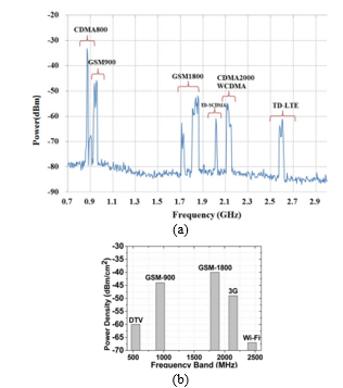
Fig. 1. RF power receive: (a) Outside shopping mall [13]; (b) Distributed RF power density in ambient [16]
2. Receiving Antenna Design
The fabricated antenna is shown in Fig. 2. The proposed antenna has dimension of 46 mm of length, 30 mm of width. The used material for substrate is Rogers RO4003 with dielectric constant of 3.55 and thickness of 0.8 mm.
This structure is inspired from the antenna design in [17,18] . Paper [18] presents a low-profile dual-band printed Inverted-L (IL) shaped monopole antenna with Parasitic Inverted-F (PIF) shaped element in the ground plane for 2.4/5.2/5.8 GHz WLAN applications, the overall size of this antenna is 40 mm x 30 mm. We can apply directly the technique in [18] to obtain an antenna operating at GSM 900 MHz and 1800 MHz, but the size of antenna will be increased considerably. Therefore, the miniaturized technique in [19] is used to reduce the size of our structure. In [19], a miniaturized antenna using meander-line strips with the overall size of 32 mm x 32 mm is presented for operating at GSM-850, GSM- 900, UMTS-2100, WiMAX-2.3 and WiMAX-3.3 bands. However, the gain of this antenna is quite low almost for all frequency bands, even negative in GSM bands. Our antenna has dual-band with gain of 1.46 dB, 1.91 dB at GSM 900 and GSM 1800.
The return loss and far-field characteristics of the developed antenna are shown in Fig. 3 and Fig. 4. As Fig. 3, the return loss of antenna between simulation and measurement are not similar.
The measurement result is not well matched at GSM 900MHz and shifted a little toward the right at GSM 1800 MHz. This can be explained that as the coupling between two meander-lines in practice weaken or lost, the meander-line for GSM 900MHz was not appropriately excited. Therefore, antenna efficiency is not as high as we expected. This aspect must be improved in the next work.
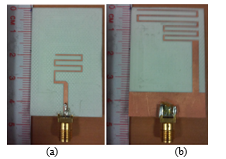
Fig. 2. Antenna prototype
(a) To view, (b) Back view
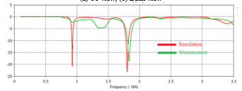
Fig. 3. Return loss of proposed antenna (red-line:simulation result; green-line: measurement result)
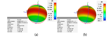
Fig. 4. Radiation patten of proposed antenna
(a) GSM 900; (b) GSM1800
3. Rectifying Circuit Design
The structure of a classical rectenna is shown in Fig. 5. A rectifier consists of a harmonic filter, an impedance matching network to maximize the power transfer from the receiving antenna to AC – to – DC conversion circuit, a conversion circuit converting the received signal by antenna to DC signal, a DC filter to smooth DC signal and to bring the harmonic signal back to rectify and a resistive load. However, this proposed rectifier does not use the Harmonic filter.
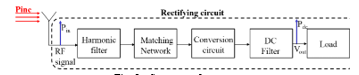
Fig. 5. Structure of rectenna
The RF signal is rectified by a voltage doubling circuit using Schottky diode. The topology of voltage double and the model of diode are shown in Fig. 6. The voltage double consists of two stages, the first one includes capacitor C1 and diode D1 clamping the negative part of input signal and the second one includes capacitor C2 and diode D2 for peak rectification. C1 is used in order to block the harmonics generated by the diode (due to its nonlinear behavior) and return to the receiving antenna to avoid the unwanted radiation. C2 plays a role as a DC filter, and also storages energy, which would be then replaced by a dual radial stub DC filter. The output voltage is defined as:![]()
Where Vout is output dc voltage, Vin is input voltage, Vd is forward voltage of diode.
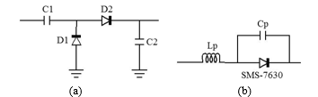
Fig. 6. (a) Voltage double circuit; (b) Diode SMS-7630 model
The diode is the most important component in the design of a rectifying circuit. As shown in paper [20], diode SMS-7630 is chosen. SPICE model parameters of diode SMS-7630 are taken from [21]. The parasitic phenomenon due to package of diode is considered by a parasitic inductor Lp = 0.7 nH and a parasitic Cp = 0.045 pF. First, the impedance matching network can be (made from?) implemented by lumped elements or distributed elements. In our project, we use a dual-stub matching network to match the receiving antenna and the rectifier at two frequencies. Fig. 7 illustrates the impedance matching network after the total size reduction by meander-line. Fig. 8 shows simulated result of matching network. The good impedance matching is achieved at GSM 900 MHz and GSM 1800 MHz, proving the capability of the dual-frequency matching circuit.
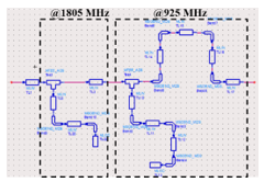
Fig. 7. Impedance matching network
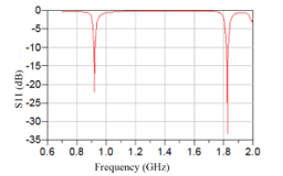
Fig. 8. Simulated result of matching network
Second, a DC filter helps smoothing the DC signal as well as bringing the harmonics back to rectify and its filtering characteristics. The DC filter with dual radial stub has the function of attenuating the fundamental frequency of GSM 900 MHz and 1800 MHz. Besides, the second and the third harmonics are well filtered with less than -3dB transmission coefficient S21 (cf. Fig. 9).
The rectifying circuit is simulated by Harmonic Balance (HB) and Large Signal S-Parameter (LSSP) simulation of ADS in . It is optimized for low input power level of -20 dBm at 925 MHz and 1805 MHz (two frequencies begin the downlink channels of GSM 900 MHz and 1800 MHz, respectively). An optimized load of 8.2kΩ is selected for maximum conversion efficiency. The Fig. 10 shows the photograph of the fabricated rectifier with the total sizes of 10 cm x 6.5 cm. The substrate Roger 4003C is used.
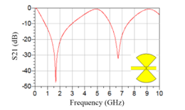
Fig. 9. DC filter and its characteristic
The measured and simulated results indicate that at the low input power level of -20 dBm, the rectifier operates at two frequencies of 925 MHz and 1805 MHz with conversion efficiency of 30.4% and 20%, and output voltage of 158 mV and 128 mV, respectively.
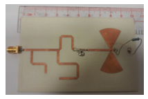
Fig. 10. Photograph of the fabricated rectifier
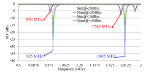
Fig. 11. Return loss of rectifier with difirent incident power level
Fig. 11 plots the measured and simulated return losses (S11) of rectifier at different input power levels. The measurement results are shifted a little toward the left and not well matched. It can be explained by two reasons. Firstly, the dielectric constant of Rogers RO4003 can vary from 3.38 to 3.55. When the dielectric constant increases, the resonant peak shifts to lower frequency. Secondly, it can be due to diode model, especially the junction capacitance Cj [20]. By increasing Cj, we find that the resonant frequency shifts to lower frequency and the power conversion efficiency degrades drastically.
Fig. 12 presents the results of efficiency and output voltage of the dual-band rectifier when varying incident power level from – 20 dBm to 5 dBm. The maximum output DC voltage is 3.3 V with an input power incident of 0 dBm. However, the incident power of GSM900 and GSM1800 can never be 0 dBm. Table I compares the simulated and measured results at the input power level of -20 dBm.
As the results are shown in Table I, the measured efficiency is haft of simulation result. The inaccurate diode model can be the reason as described above. However, this circuit gives the acceptable output voltage with the low input power level. The exact diode is expected to give higher power conversion efficiency.
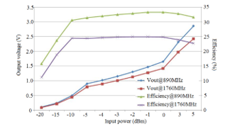
Fig. 12. Efficiency and ouput voltage of rectifier
TABLE I. COMPARISON OF SIMULATION AND MEASUREMENT OF RECTIFIER WITH Pin = -20dBm
| Frequency(GHz) | Efficiency (%) | Out voltage (mV) | |
| Sim |
0.925 1.805 |
30.4 20 |
158 128 |
| Meas |
0.890 1.760 |
15.8 11.2 |
114 96 |
4. Rectenna performance
The receiving antenna and rectifier are designed and evaluated separately. Then they are integrated into the rectenna prototype that is fabricated and evaluated, as presented in Fig. 13:
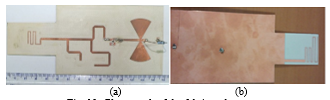
Fig. 13. Photograph of the fabricated rectenna
(a) Top view; (b) back view
The rectenna measurement is performed in an anechoic chamber as in Fig. 14. The receiving antenna is fixed in front of the transmitting antenna, the received RF power of antenna, PRF, will be measured by spectrum analyzer. After that, the receiving antenna will be replaced by rectenna at the same position, the output voltage of rectenna (Vout) will be measured by a voltmeter. The conversion efficiency of rectenna ηRF-DC is defined as the ratio of the DC power PDC and the RF power PRF:![]()
The results of rectenna are presented in Fig. 15 and Fig. 16. Our rectenna recovers the voltage from 183 mV to 415 mV when it is placing near the mobile and in ambient environment (cf. Fig. 16). The efficiency of rectenna is 40.8% and 20% at 1834 MHz and 890 MHz, respectively, with incident power of – 20 dBm.
Table II shows the comparison of various rectifiers published in several literatures. This work provides a dual-band design with higher conversion efficiency. As observed from the table, this work provides a dual-band design with higher conversion efficiency compared to others at the input power level of -20 dBm. However, the total size is bigger than [16,22-24] and smaller than [7] because of the large dimension of DC filter and dual-band coplanar receiving antenna.
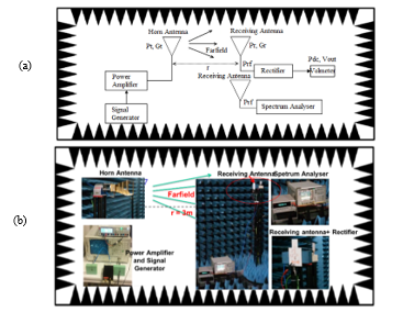
Fig. 14. Rectenna measurement setup in the anechoic chamber at IMEP-LAHC laboratory
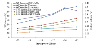
Fig. 15. Measured output voltage versus input power of only-rectifier and rectenna
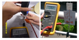
Fig. 16. Rectenna experimen in ambient environement
Table II. COMPARISON OF THE PROPOSED RECTENNA AND THE RELATED WORKS
| Ref |
Freq (GHz) |
Diode |
Input power (dBm) |
η (%) |
Total sizes*
|
| [7] |
1.8 2.5 |
HSMS285C | -20 | 33.5 | 0.72 x 0.57 |
| [22] | 0.915 | HSMS2860 | -17 | 40 | 0.14 x 0.13 |
| [16] |
0.915 1.8 |
HSMS 2850 | -15 to 20 | >30 | 0.17 x 0.1 |
| [23] | 2.45 | SMS 7630 | -20 | 27.7 | 0.37 x 0.33 |
| [24] |
1.8 2.45 |
SMS 7630 | -20 | 13 | 0.5 x 0.5 |
|
This work |
0.925 1.805 |
SMS 7630 | -20 | 20 to 40.8 | 0.67 x 0.27 |
|
N/a is not available η is conversion efficiency of rectenna * is the distance calculated by the wavelength |
|||||
The rectenna efficiency is quite high compared to rectifier efficiency at section 3. This can be explained by the effect of ground layer of rectifier to monopole antenna performance when the antenna is integrated into rectifier. This aspect is being discussed and reviewed in our current research. Nonetheless, these results demonstrate the potential application of this rectenna in autonomous sensor or self-powered electronic device where additional storage of energy circuit is required.
5. Conclusion
A dual-band rectenna was designed and tested in ambient environment. Simulation results show that the presented rectenna can achieve good voltage. Measurement results on a prototype rectenna show that the operating frequency was well-matched; the rectenna harvests the maximum of 415 mV in ambient environment, which implies that the proposed rectenna is suitable for autonomous sensor application. However, as we mentioned in Section 2, the receiving antenna of this rectenna can be optimized in the future researches to give higher efficiency. A super capacitor can be inserted into the circuit to store energy that is harvested by our rectenna.
Acknowledgment
This research is funded by Ministry of Education and Training (MOET) under grant number B2015-01-93.
- S. Kim et al., ‘Ambient RF Energy-Harvesting Technologies for Self-Sustainable Standalone Wireless Sensor Platforms’, Proc. IEEE, vol. 102, no. 11, pp. 1649–1666, Nov. 2014.
- G. Andia Vera, A. Georgiadis, A. Collado, and S. Via, ‘Design of a 2.45 GHz rectenna for electromagnetic (EM) energy scavenging’, 2010, pp. 61–64.
- R. A. Rahim, S. I. S. Hassan, F. Malek, M. N. Junita, and M. F. Jamlos, ‘An investigation of ambient radio frequency as a candidate for energy harvesting source’, 2012, pp. 95–99.
- R. Scheeler, S. Korhummel, and Z. Popovic, ‘A Dual-Frequency Ultralow-Power Efficient 0.5-g Rectenna’, IEEE Microw. Mag., vol. 15, no. 1, pp. 109–114, Jan. 2014.
- K. Niotaki, S. Kim, S. Jeong, A. Collado, A. Georgiadis, and M. M. Tentzeris, ‘A Compact Dual-Band Rectenna Using Slot-Loaded Dual Band Folded Dipole Antenna’, IEEE Antennas Wirel. Propag. Lett., vol. 12, pp. 1634–1637, 2013.
- H. Sun, Y. Guo, M. He, and Z. Zhong, ‘A Dual-Band Rectenna Using Broadband Yagi Antenna Array for Ambient RF Power Harvesting’, IEEE Antennas Wirel. Propag. Lett., vol. 12, pp. 918–921, 2013.
- S. S. Sarma and M. J. Akhtar, ‘A dual band meandered printed dipole antenna for RF energy harvesting applications’, 2016, pp. 93–94.
- S. Keyrouz, H. J. Visser, and A. G. Tijhuris, ‘Multi-band simultaneous radio frequency energy harvesting’, presented at the 7th European Conference on Antennas and Propagation, Gothenburg, Sweden, 2013.
- M. Arrawatia, M. S. Baghini, and G. Kumar, ‘Broadband rectenna array for RF energy harvesting’, 2016, pp. 1869–1870.
- M. Arrawatia, M. Baghini, and G. Kumar, ‘Broadband Bent Triangular Omnidirectional Antenna for RF Energy Harvesting’, IEEE Antennas Wirel. Propag. Lett., pp. 1–1, 2015.
- Hongxian Zhang and Xinen Zhu, ‘A broadband high efficiency rectifier for ambient RF energy harvesting’, 2014, pp. 1–3.
- N. Shariati, W. S. T. Rowe, J. R. Scott, and K. Ghorbani, ‘Multi-Service Highly Sensitive Rectifier for Enhanced RF Energy Scavenging’, Sci. Rep., vol. 5, p. 9655, May 2015.
- A. S. Andrenko, Xianyang Lin, and Miaowang Zeng, ‘Outdoor RF spectral survey: A roadmap for ambient RF energy harvesting’, 2015, pp. 1–4.
- J. Tavares et al., ‘Spectrum opportunities for electromagnetic energy harvesting from 350 mhz to 3 ghz’, 2013, pp. 126–130.
- M. Pinuela, P. D. Mitcheson, and S. Lucyszyn, ‘Ambient RF Energy Harvesting in Urban and Semi-Urban Environments’, IEEE Trans. Microw. Theory Tech., vol. 61, no. 7, pp. 2715–2726, Jul. 2013.
- Z. Liu, Z. Zhong, and Y.-X. Guo, ‘Enhanced Dual-Band Ambient RF Energy Harvesting With Ultra-Wide Power Range’, IEEE Microw. Wirel. Compon. Lett., vol. 25, no. 9, pp. 630–632, Sep. 2015.
- ‘Advanced Design System (ADS) | Keysight (formerly Agilent’s Electronic Measurement)’. [Online]. Available: http://www.keysight.com/en/pc-1297113/advanced-design-system-ads?cc=VN&lc=eng. [Accessed: 02-Mar-2017].
- C. G. Permana and A. Munir, ‘Printed multiband antenna for mobile and wireless communications’, 2011, pp. 236–240.
- S. Verma and P. Kumar, ‘Printed inverted-L shaped monopole antenna with Parasitic Inverted-F element for dual band applications’, Microw. Opt. Technol. Lett., vol. 56, no. 5, pp. 1163–1167, May 2014.
- ‘Harvesting Wireless Power: Survey of Energy-Harvester Conversion Efficiency in Far-Field, Wireless Power Transfer Systems’, IEEE Microw. Mag., vol. 15, no. 4, pp. 108–120, Jun. 2014.
- ‘SKYWORKS: Products: SMS7630 Series’. [Online]. Available: http://www.skyworksinc.com/Product/511/SMS7630_Series. [Accessed: 27-Oct-2016].
- A. M. Almohaimeed, M. C. E. Yagoub, and R. E. Amaya, ‘Efficient rectenna with wide dynamic input power range for 900 MHz wireless power transfer applications’, 2016, pp. 1–4.
- T. J. Lee, P. Patil, C. Y. Hu, M. Rajabi, S. Farsi, and D. M. M.-P. Schreurs, ‘Design of efficient rectifier for low-power wireless energy harvesting at 2.45 GHz’, 2015, pp. 47–49.
- C. Song, Y. Huang, J. Zhou, J. Zhang, S. Yuan, and P. Carter, ‘A High-Efficiency Broadband Rectenna for Ambient Wireless Energy Harvesting’, IEEE Trans. Antennas Propag., vol. 63, no. 8, pp. 3486–3495, Aug. 2015.