L-Band SiGe HBT Active Differential Equalizers with Variable, Positive or Negative Gain Slopes Using Dual-Resonant RLC Circuits
L-Band SiGe HBT Active Differential Equalizers with Variable, Positive or Negative Gain Slopes Using Dual-Resonant RLC Circuits
Volume 2, Issue 3, Page No 362-368, 2017
Author’s Name: Yasushi Itoha), Hiroaki Takagi
View Affiliations
Shonan Institute of Technology , Electrical and Information Engineering, 251-8511, Japan
a)Author to whom correspondence should be addressed. E-mail: itoh@elec.shonan-it.ac.jp
Adv. Sci. Technol. Eng. Syst. J. 2(3), 362-368 (2017); ![]() DOI: 10.25046/aj020346
DOI: 10.25046/aj020346
Keywords: Microwaves, Active Equalizer, Differential Amplifier

Export Citations
L-band SiGe HBT active differential equalizers with variable, positive or negative gain slopes have been designed and fabricated for frequency and temperature compensation of microwave and optical systems. The active equalizer employs dual-resonant RLC circuits in the series feedback path of the differential amplifier for positive gain slopes or in the load for negative gain slopes. The implemented active equalizers have achieved positive gain slopes of +54 to +87dB/GHz across 0.2 to 0.6GHz as well as negative gain slopes of -50 to -100dB/GHz over 0.6 to 1.2GHz. The active differential equalizers presented in this paper have an outstanding feature of providing variable, positive or negative gain slopes, which can be easily adjusted to meet with various stringent requirements for frequency and temperature compensation in microwave and optical systems.
Received: 01 April 2017, Accepted: 02 May 2017, Published Online: 17 May 2017
1. Introduction
First of all, this paper is an extension of the work originally presented in the 46th European Microwave Conference, 2016 [1]. The research and development of active equalizers have started at the beginning of 1970s as active RC filters with IC operational amplifiers in the audio band because of having many advantages over passive equalizers in terms of inductor-less, cheaper, smaller, easily manufactured and tuned circuits [2]. Since then, various types of active, adjustable amplitude and delay equalizers have been developed, including classical Bode variable equalizers, transfer-function types and switched-capacitor equalizers [3, 4, 5]. With the tremendous growth in semiconductor NMOS, CMOS devices, the R&D activities of active equalizers have moved toward wideband, high speed data transmission systems, a variety of analog adaptive equalizer architectures have been developed to eliminate signal distortions [6, 7, 8, 9]. Meanwhile, wideband microwave and optical receivers have been long tackled with the pass-band negative gain slope due to the falling off of gain of transistors and the insertion loss of passive elements as frequency increases [7, 10]. To address this issue, several types of passive equalizers have been reported, having fixed positive or negative gain slope as a function of frequency [11]. In addition, to realize the adjustability for the required gain slopes, a variety of active equalizers using diodes or transistors have been reported, having variable positive or negative gain slopes [10, 12, 13]. Although these circuits employ active devices, the circuit configuration is basically a passive type where fixed capacitances are replaced by diodes or transistors to provide variable gain slopes. Therefore, the insertion loss is seriously large. To address this problem, the authors have presented various types of the active equalizer with variable, positive or negative gain slopes. The advanced feature is in that active devices are used as an amplifier in place of the conventional switching or variable-capacitance device to achieve high gain. Moreover, to achieve higher frequency operation as well as miniaturized size, LC-resonators in place of the traditional RC filters are employed in the series feedback path or load circuit of the differential amplifier for positive or negative gain slopes. The active differential equalizers are as follows: Capacitance-selectable bridged-T attenuators were incorporated into the series feedback path to achieve variable positive gain slopes, which can be digitally controlled [14]. Series LC resonators were employed in the base or collector bias circuits to realize variable, positive or negative gain slopes [15]. Single-band series or parallel LC resonators were used in the feedback path of the differential amplifier for the same purposes [16]. These active equalizers, however, can vary gain slopes but the frequency positions were fixed. To overcome this problem, a novel active differential equalizer having variable inclination and position of the positive or negative gain slopes have been presented in [1]. It employs dual-resonant RLC circuits in the feedback path of the differential amplifier for positive gain slopes or in the load for negative gain slopes. To extend the work, the theory and design for the active differential equalizer using the dual-resonant RLC circuits are described in more detail. Then the circuit design, simulation and performance are newly added for the case that dual capacitors (actually two varactor diodes) consisting of the dual-resonant RLC circuit are independently varied. These active differential equalizers are relatively narrowband as well as provide abrupt gain slopes but can be easily extended to wideband design with the proper choice of circuit parameters.
2. Active Differential Equalizer Using Dual-Resonant RLC Circuits
Two types of the active differential equalizers with variable inclination and position of the positive or negative gain slopes are graphically shown in Figure 1. fPP and fPN are peak frequencies. fBP and fBN are bandstop frequencies. The conventional active equalizers [14, 15, 16] can vary either a peak or bandstop frequency. Thus only gain slope can be varied. On the other hand, the novel active equalizers can vary both peak and bandstop frequencies. Thus both the inclination and position of gain slopes can be varied.
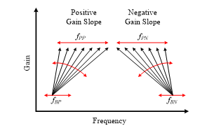
Figure 1 Two types of the active differential equalizers with variable inclination and position of the positive or negative gain slopes
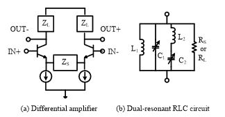
Figure 2 Schematic diagram of the differential amplifier and dual-resonant RLC circuit
Schematic diagrams of the differential amplifier and dual-resonant RLC circuit are shown in Figure 2. The dual-resonant circuit consists of series LC (L2, C2) and parallel LC (L1, C1) circuits combined with a resistor (RS or RL). The dual-resonant RLC circuit becomes purely resistive at the frequency f1 and f2, which are given as follows: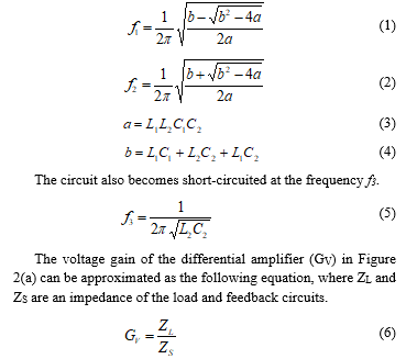
When the dual-resonant RLC circuit is applied to ZS, GV becomes minimum at f1 and f2 as well as maximum at f3, which is graphically shown in Figure 3(a). Whereas, when the dual-resonant RLC circuit is applied to ZL, GV becomes maximum at f1 and f2 as well as minimum at f3, which is graphically shown in Figure 3(b). The differential amplifier provides variable, positive gain slopes (GP) between f1 and f3 by adjusting f1 or f3. Actually, f1 or f3 can be varied with C1 or C2. It must be noted here that both f1 and f3 can be varied with C1. Meanwhile, the differential amplifier produces variable, negative gain slopes (GN) between f1 and f3 by adjusting f1 or f3. In the similar way, f1 or f3 can be varied with C1 or C2. However, it must be also noted that both f1 and f3 can be varied with C1.
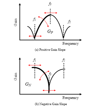
Figure 3 Voltage gains of the differential amplifier when the dual-resonant RLC circuit is applied to ZS or ZL.
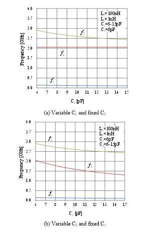
Figure 4 Calculated resonant frequencies f1, f2 and f3
Table 1 Circuit element values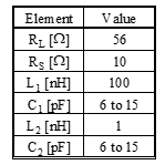
The resonant frequencies f1, f2 and f3 are calculated by using (1) to (5) and are shown in Figure 4. The circuit element values are listed in Table 1. It is clearly shown that the inclination and position of positive or negative gain slopes can be tuned by varying C1, C2 or both. As described above, f1 and f3 cannot be varied independently with C2 changes in Figure 4(b).
3. Circuit Design
Schematic diagrams of the active differential equalizer with variable, positive or negative gain slopes are displayed in Figures 5 and 6, respectively. Dual-resonant RLC circuits are employed in the feedback path of the differential amplifier for positive gain slopes or in the load for negative gain slopes.
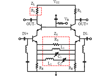
Figure 5 Schematic diagram of the active differential equalizer with variable, positive gain slopes
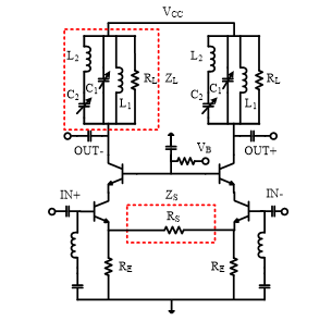
Figure 6 Schematic diagram of the active differential equalizer with variable, negative gain slopes
As shown in Figure 2(b), the dual-resonant RLC circuit consists of a series LC circuit (L2, C2), a parallel LC circuit (L1, C1) and a resistor (RS or RL). RS or RL plays an important role of circuit stability and impedance matching. RL is basically chosen as 50 ohms for impedance matching. But RS has to be carefully determined to achieve both high stability and high gain. When the dual-resonant RLC circuit is employed in ZS, RL is used in ZL. Meanwhile, the dual-resonant RLC circuit is employed in ZL, RS is utilized in ZS.
Now the voltage gain with positive gain slopes (GP) and that with negative gain slopes (GN) can be given from (6) as follows: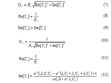
GP and GN are calculated by using (7) to (12) and the circuit element values in Tables 1. The calculation was done for variable C1 and fixed C2 or variable C2 and fixed C1. The calculated GP and GN are plotted in Figures 7 and 8, respectively. It is clearly demonstrated that variable, positive or negative gain slopes can be obtained. Due to a large value of L1, a variation of the bandstop frequency f1 is small in Figure 7. Thus the positive gain slopes greatly change with f2 (C2) in Figure 7(b). In the similar way, due to a large value of L1, a variation of the bandstop frequency f1 is also small in Figure 8. The negative gain slopes largely vary with f2 (C2) in Figure 8(b).
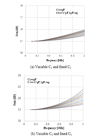
Figure 7 Calculated GP for variable C1 and fixed C2 or variable C2 and fixed C1
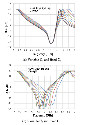
Figure 8 Calculated GN for variable C1 and fixed C2 or variable C2 and fixed C1
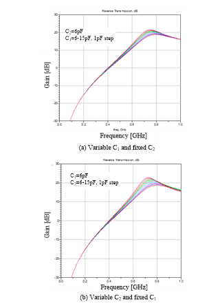
Figure 9 Simulated gains of the active differential equalizer with variable, positive gain slopes
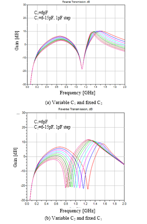
Figure 10 Simulated gains of the active differential equalizer with variable, negative gain slopes
4. Circuit Simulation
Based on the schematic diagrams of Figures 5 and 6, the circuit simulation was accomplished by using ADS. A cascode connection of SiGe HBTs is employed to control gain. In order to improve input and output matching, reactive elements of L and C are employed in the input matching circuit as well as the value of RL was determined as 56 ohms. The value of RS was finally chosen as 10 ohms to keep high gain and stabilize the circuit. The simulation was done for variable C1 and fixed C2 or variable C2 and fixed C1. The simulated gains of the active differential equalizer with variable, positive or negative gain slopes are plotted in Figures 9 and 10, respectively. The variation of positive gain slopes is a little bit larger for f3 (C2) changes, which is in good agreement with Figures 4 and 7. In the similar way, the variation of negative gain slopes is also larger for f3 (C2) changes. In Figure 10(b), both the inclination and position of negative gain slopes have drastically changed.
5. Circuit Fabrication
Photographs of the active differential equalizer with variable, positive or negative gain slopes are shown in Figure 11. The active differential equalizers were fabricated on the FR-4 substrate with a dielectric constant of 4.5. 0.35mm SiGe HBTs with an ft of 25GHz (Toshiba MT4S102T), 1005-type resistors, inductors and capacitors are mounted on the substrate by soldering. A surface mount type of the varactor diode with a capacitance ratio of 2.5 (Toshiba 1SV279) was used. The circuit size is 14 x 16 x 1.2 mm3.
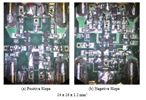
Figure 11 Photographs of the active differential equalizer with variable, positive or negative gain slopes
6. Circuit Performance
The measured gains of the active differential equalizers are plotted in Figure 12 for the positive gain slopes and in Figure 13 for the negative gain slopes. The measurement was done for variable C1 and fixed C2 or variable C2 and fixed C1. Actually C1 or C2 was varied with a control voltage VC1 or VC2 of the varactor diode. The measurement conditions are shown in Figures 12 and 13, respectively.
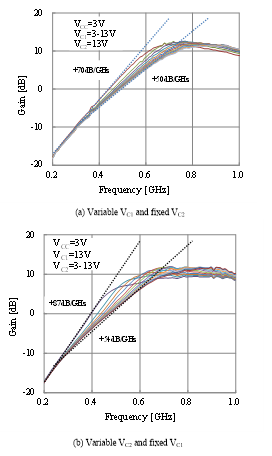
Figure 12 Measured gains of the active differential equalizer with variable, positive gain slopes
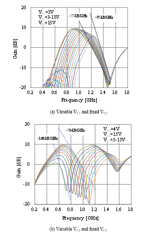
Figure 13 Measured gains of the active differential equalizer with variable, negative gain slopes
The active differential equalizer with variable, positive gain slopes has achieved a gain slope of +50 to +70dB/GHz over 0.2 to 0.6GHz in Figure 12(a) as well as +54 to +87dB/GHz across 0.2 to 0.6GHz in Figure 12(b). The input and output return losses were better than 2dB and 15dB, respectively, which can be easily improved by employing a lossy match circuit in the input matching circuit.
The active differential equalizer with variable, negative gain slopes has achieved a gain slope of -55 to -95dB/GHz over 1.1 to 1.5GHz in Figure 13(a) as well as -50 to -100dB/GHz across 0.6 to 1.2GHz in Figure 13(b). The input and output return losses were better than 2dB. In a similar way as the positive gain slope, the input and output matches can be further improved with the use of a lossy match configuration.
These performances were compared with the conventional active equalizers and summarized in Table 2. It is clearly shown that the active differential equalizers presented in this paper can provide narrow-band but abrupt gain slopes as well as higher gain. With the proper choice of the circuit parameters, it is very easy to meet with the moderate gain slopes over a wide bandwidth.
Table 2 Summary of performances of active equalizers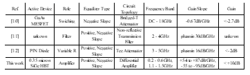
7. Conclusions
Two types of the active differential equalizers with variable, positive or negative gain slopes have been presented. With the use of the dual-resonant RLC circuit in the feedback or load circuit, the active differential equalizers have achieved positive gain slopes of +54 to +87dB/GHz across 0.2 to 0.6GHz as well as negative gain slopes of -50 to -100dB/GHz over 0.6 to 1.2GHz. The active differential equalizers presented in this paper show narrow bandwidth but abrupt gain slopes, which can be easily extended to wide bandwidth and moderate gain slopes with the proper choice of the circuit parameters. Moreover, the input and output matches can be improved with the use of a lossy match structure. It can be concluded from these results that the active differential equalizers would be one candidate for frequency and temperature compensations in microwave and optical systems.
- Y. Itoh and H. Takagi, “L-Band SiGe HBT Active Differential Equalizers with Variable Inclination and Position of the Positive and Negative Gain Slopes”, Proceeding of the 46th European Microwave Conference, pp. 1015-1018, October 2016
- Paul E. Fleischer, “Active Adjustable Loss and Delay Equalizers”, IEEE Trans. Circuits and Systems, vol.CAS-21, No. 4, pp. 527-531, July 1974.
- Franc Brglez, “Minimally Active RC Variable Equalizers”, IEEE Trans. Circuits and Systems, vol.CAS-22, No. 8, pp. 688-691, August 1975.
- Robert R. Cordell, “A New Family of Active Variable Equalizers”, IEEE Trans. Circuits and Systems, vol.CAS-29, No. 5, pp. 316-322, May 1982.
- Antonio Petraglia and Sanjit K. Mitra, “Switched Capacitor Equalizers with Digitally Programmable Tuning Characteristics”, IEEE Trans. Circuits and Systems, vol.CAS-38, No. 11, pp. 1322-1331, November 1991.
- Tadayoshi Enomoto, Kasaaki Yasumoto, Tsutomu Ishihara and Kohjiro Watanabe, “Monolithic Analog Adaptive Equalizer Integrated Circuit for Wide-Band Digital Communication Networks”, IEEE Journal of Solid-State Circuits, vol.SC-17, No. 6, pp. 1045-1054, December 1982.
- K. W. Goossen, J. A. Walker, D. T. Neilson, J. E. Ford and W. H. Knox, “Micromechanical Gain Slope Compensator for Spectrally Linear Optical Power Equalization”, IEEE Photonics Technology Letters, Vol. 12, No. 7, pp. 831-833, 2000.
- H. Kim, F. Bien, S. Chandramouli, J. Cha, E. Gebara and J. Laskar, “A 0.25-um BiCMOS Feed Forward Equalizer Using Active Delay Line for Backplane Communication”, IEEE Symposium on Circuits and Systems, pp. 193-196, May 2007.
- Melikyan Vazgen Sh.,, Sahakyan Arthur S., Safaryan Karo H., Dingchyan Hayk H.,, “High Accuracy Equalization Method for Receiver Active Equalizer”, Proceeding of the East-West Design & Test Symposium, 2013
- H. J. Sun and B. C. Morley, “A DC-18GHz GaAs MESFET Monolithic Variable Slope Gain-Equalizer IC”, IEEE 1989 Microwave and MMW Monolithic Circuit Symposium Digest, pp. 79-82.
- H. Wang, B. Yan, Z. Wang and R. Xu, “A Broadband Microwave Gain Equalizer”, Progress in Electromagnetic Research Letters, Vol. 33, pp. 63-72, 2012.
- S. C. Bera, “Amplitude Tilt Active Equalizer for Frequency and Temperature Compensation”, IEEE Microwave and Wireless Component Letters, Vol. 21, No. 7, pp. 344-346, 2011.
- M Morgan, T. Newton, T. B. Hayward, and T. Boyd, “Non-Reflective Transmission-Line Filters for Gain Slope Equalization”, 2007 IEEE/MTT-S International Microwave Symposium Digest, pp. 545 – 548.
- Y. Itoh, N. Mizuo and A. Ohta,” An L-Band 4-bit SiGe HBT Active Differential Equalizer Using Capacitance-Selectable Bridged-T Attenuators”, Proceeding of the ISMOT 2015, pp.164 -166, June 2015.
- Y. Itoh and H. Takagi, “L-Band SiGe HBT Active Differential Equalizers with Varactor-Tuned Bias Circuits for Variable Positive or Negative Gain Slopes”, Contemporary Sciences, Vol. 9, No. 15, pp. 727-733, 2016.
- Y. Itoh and H. Takagi, “L-Band SiGe HBT Active Differential Equalizers Providing Variable Positive or Negative Gain Slopes”, Proceeding of the 21th International Conference on Microwaves, Radar and Wireless Communications, May 2016.