COTS – Harsh Condition Effects Considerations from Technology to User Level
COTS – Harsh Condition Effects Considerations from Technology to User Level
Volume 2, Issue 3, Page No 1592-1598, 2017
Author’s Name: Kirsten Weide-Zaage1, a), Guillermo Payá-Vayá2
View Affiliations
1RESRI Group, Institute of Microelectronic Systems, Leibniz Universität Hannover, 30176, Hannover, Germany
2AS Group, Institute of Microelectronic Systems, Leibniz Universität Hannover, 30176, Hannover, Germany
a)Author to whom correspondence should be addressed. E-mail: weide-zaage@ims.uni-hannover.de
Adv. Sci. Technol. Eng. Syst. J. 2(3), 1592-1598 (2017); ![]() DOI: 10.25046/aj0203198
DOI: 10.25046/aj0203198
Keywords: Radiation, Simulation, SRAM, Metallization, Reliability, Migration, Packaging, Circuit

Export Citations
Radiation hardened devices are mostly extremely expensive. The continuously downscaling of microelectronic structures and the unavoidable presence of particle radiation on ground and in space leads to unwanted failures in electronic devices. Furthermore it is expected that in the next few years around 8000 new satellites will be launched around the world. Due to the enormous increasing need for Rad-Hard devices, there will be more focus on Commercial Of The Shelf (COTS) devices, which costs are lower. Also nowadays microelectronics for automotive systems are tested to withstand radiation especially SEU-single event upsets. It is clear that SEU cannot be ignored anymore especially in the application of unmanned autonomous vehicles and systems. Reliability testing is expensive and extremely time consuming. The use of COTS-Commercials of the shelf is the ultimate goal to reach. In this paper, an overview of radiation effects on different CMOS technologies used in COTS devices is given. These effects can be considered while selecting different functional equivalent COTS devices implemented with different technologies. Moreover, an overview of software techniques used in programmable commercial devices to reduce the radiation effects is also described.
Received: 15 June 2017, Accepted: 23 July 2017, Published Online: 24 August 2017
1. Introduction
This paper is an extension of work originally presented at the SMTA Pan Pacific Symposium [1].
It is well known, that CMOS components are radiation sensitive and mostly have a variability concerning radiation response. The most commercial devices can withstand doses in the order of 5-10 krad and a minority can survive up to 100 krad [2]. To identify the more Rad-Hard Components radiation tests are needed. To get information about the radiation response especially single event upsets (SEU), the influences of the technology node, metallization scheme, new materials as well as package and shielding materials have to be investigated and evaluated. It has to be said, that concerning packaging materials, design and technology many steps were taken to avoid radiation sensitivity.
Ideally, the purchaser would like to have a homogeneous quantity for the purchase of several components, which originate from the same process line produced simultaneously. Then the characterization of the radiation behavior of a small sample of parts is representative for the whole lot. In cases where the contract volume is interesting for the trader or manufacturer, it may be possible to negotiate a better traceability with the manufacturer / trader. Another possibility is the use of qualified automotive components for space applications. Here the problem is that air and space applications have almost smaller quantities compared to automotive and the manufacturers only deliver big quantities.The procurement of COTS parts for use in a radiation environment is a problem. Technically the same components are produced in different foundries of the companies. A product can be changes without the knowledge of the consumer if the datasheet is not affected.
The increase of high integration of chip and package influences the costs and the time-to-market in parts negatively. The system complexity results in integration of analog and digital components on a single chip and the use of new packaging concepts.
The environment as well as new materials like Pb-free solder or Platinum as metallization material, the use of organic materials and new dielectrics influence the reliability and quality of the devices and systems and can yield, in the worst case, to a complete re-design (Figure 1).
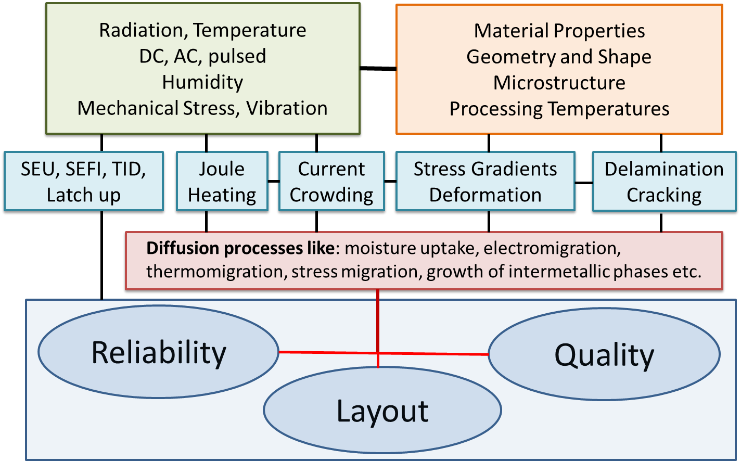 Figure 1. Reliability, quality and layout dependence of some physical failures in the devices and components.
In this paper several considerations about radiation effects are given in Section 2. After the description of the different CMOS related failures and a discussion of the different technology and materials, some simulation ideas will also be considered in the frame of high temperature application. Furthermore migration effects resulting from harsh conditions are discussed. Looking to ultra-scaled memories, it is found that the sensitivity against radiation is directly coupled with the reduction of the size and the distance between two circuits. This leads directly to a reduction of the critical charge which can induce a bit flip [3]. Then section 3 introduces different methods used in programmable COTS devices to reduce or mitigate the harsh condition effects. Finally this paper is concluded in Section 4.
2. Technology Node and Material
The quantity of products from the different technology nodes is shown in Figure 2. It is found, that a big portion of the products is still manufactured in 180 nm and 130nm technology node [4].
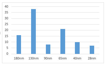 Figure 2. Quantity of products in (%) of the different technology nodes.
Generally the number of the materials used in the Front-End manufacturing of the devices is in the two-digit range. Every material and processing step can have more or less influence on the radiation sensitivity of the device. A look on the semiconductor processing as well as the materials and the packaging for the technology nodes beyond the 65nm node is necessary caused by the fact that materials etc. change. In the 22nm technology node with Hafnium as gate material new possible radiation risks may occur. 174Hf is an alpha particle emitter. Materials used in the semiconductor industry with their natural occurrence are shown in Table 1. An investigation of SEU related to these materials shows that due to the high half-life there should not be a problem. However, due to the ultra-high integration the portion of these material increases drastically and therefor an SEU risk cannot be excluded anymore.
Table 1. Alpha-Emitter with half-live and natural occurrence.
| Alpha Emitter | Half-live (a) | Natural occurrence [%] |
| 174Hf | 2.0 x 10¹⁵ | 0.162 |
| 152Gd | 1.08 x 10¹⁴ | 0.2 |
| 144Nd | 2.29 x 10¹⁵ | 23.8 |
| 148Sm | 7.0 x 10¹⁵ | 11.3 |
| 147Sm | 1.06 x 10¹¹ | 15.0 |
| 90Pt | 6.5 x 10¹¹ | 0.01 |
2.1. Alpha Particles and Packaging
The emissivity of alpha particles in the different package materials are given in Table 2 [4-8]. Especially in Flip-Chip applications the emissivity’s as well as the range in the materials are important. The highest emissivity is found in Pb based solder followed by Sn based solder material.
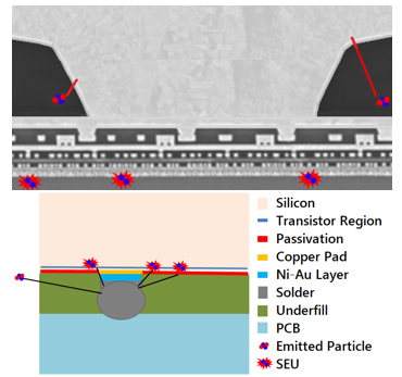 Figure 3. Schematic view of the interaction between particles emitted from the solder with the transistor level.
In Figure 3 the interaction between particles emitted from the solder with the transistor level is shown schematically. The risk for alpha emission from the Sn is not eliminated due to the fact that trace contamination of Pb in Sn occurs which cannot eliminated easily [9].
Table 2. Emissivity (α/cm²-hr) of different materials.
| Material | Emissivity (α/cm²-hr) |
| Mold Compound | 0.024à < 0.002 |
| Underfill Flip Chip Pb | 0.004à 0.0007 |
| Eutectic Pb based Solder | 7300à < 0.0009 |
| DIP Leadframe | 0.00677 |
| Alloy 42 (Hitachi) | 8 |
| Au-plated Alloy 42 | 4 |
| Sn | >1000 à <1 |
| AlSiC (Lanxide) | 215 |
| ZIP Leadframe | 0.00258 |
| 256K DIP | 0.00124 |
| 64K DIP | 0.00109 |
| Metal package lid | 0.030 |
| Ceramic package lid | 3.10 |
| Plastic (Epoxy) | 0.00080 |
| Ceramic DIP | 0.03230 |
| Ceramic LCC | 0.02530 |
With concern to alpha particle induced SEU several conditions must be fulfilled so that an alpha particle causes a soft error. These are:
- An alpha particle-emitting radioisotope must be present in the packaging material and at a distance within 50μm.
- The alpha particle must be emitted in the direct direction to the active layer.
- The alpha particle must have enough energy or exceed the critical charge in order to influence the active layer in such a way that a bit flip occurs.
Alternatively, the influence of the alpha particles can be eliminated by:
- a better design, i.e. more distance to the active layer
- shielding material such as die coatings or thin polyimide films
- the choice of Ultra-Low-Alpha housing materials
There are different package categories defined related to radiation. The categories are given in Table 3 [10].
Table 3. Categories of the different packages related to radiation.
| Category | Emissivity (α/cm²-hr) |
| Standard | 10 – 0.01 |
| Low-alpha (LA) | < 0.01 |
| Ultra-low-alpha (ULA) | < 0.001 |
| Hyper-low-alpha (HLA) | < 0.0005 |
2.2. CMOS Related Failure Mechanism
The following error mechanisms can be distinguished in CMOS devices:
- SEU: Single Event Upset as a singular event temporarily interfering with the system, e.g. wrong calculation information or a bit flip in a memory. If the bit is corrected, the system continues to operate normally.
- SEFI: Single Event Functional Interrupts occurring in control loops and bringing the system to an undefined state, a test mode, or a standstill that should be reset by a reset.
- SEL: In a single-event latch-up of a parasitic PNPN structure, a high-energy particle can cause a short between two transistors. This remains as long as the system is connected to the power supply. If the current is switched off and the system is restarted, the SEL is over. The energy for an SEL at the processor is 80 MeV/cm²/mg and in the CMOS-RAM 50 MeV/cm²/mg.
- SET: A single-event transient is a high-energy particle that induces a surge current that travels through the circuit and can disturb the module in a manner similar to an electrostatic discharge (ESD).
- Single event snapback, which can occur similarly to the SEL but does not require a PNPN structure.
- TID total ionizing can as a long-term impact on CMOS chips by trapping holes near the boundary layer between the dielectric (SiO2) and silicon.
2.3. Simulation of Iteration
A precise prediction of the radiation response in the new technologies and circuits is crucial to ensure a trouble-free operation. Simulation may support this and help to reduce the costs in terms of stress tests. Three dimensional physical simulations of ionizing radiation effects in the semiconductor structure, which are coupled to an external circuit simulator are one way to do so [11].
The reaction on a radiation event is in technology nodes beyond 100nm closely related to the structure of the device caused by the presence of interconnects, bias, and different metallization layers affecting the performance [11-13].
A physical-based modeling approach that includes detailed high-energy physics-based simulations of nuclear reactions coupled with advanced component and circuit simulators is a need here. With tools such as e.g. GEANT4, a refinement of TCAD simulations with e.g. SILVACO can be done. Approaches to this are described in [14, 15].
GEANT4 is an on C++ based open source software package composed of tools that can be used to simulate the interaction of particles with matter. This software package was developed at CERN. The calculation of decay, track, energy of the particles, elastic and inelastic bumps etc. is possible. Furthermore beside NIST (National Institute of Standards) materials user materials can be defined.
A Monte Carlo simulation using GEANT4 to determine the path of the particles through the transistor as well as the deposited energy was carried out. This data was then used to determine the generation rate for electron hole pairs (3.6 eV) and the radial distribution. The radial distribution is energy-dependent and complex analytical models can be used for their determination [16]. In the following simulation with the TCAD Tool SILVACO, the resulting characteristics can then be determined. In Figure 4 the simulation flow in terms of radiation using GEANT4 and SILVACO TCAD is shown.
It has to be remarked that GEANT4 is highly complex and requires a long training period and knowledge about the physics and coupling. All user interfaces have to be programmed for the special needed cases. This makes it’s use for a fast application uncomfortable.
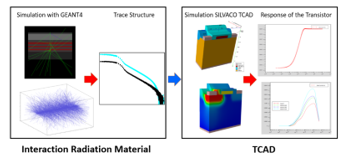 Figure 4. Simulation flow in terms of radiation.
2.4. Multilevel Metallization for Harsh Application
In CMOS devices used under harsh temperature environment tungsten metallization is used. To determine the reaction of the tungsten metallization layer on neutron radiation a metallization scheme was modeled (Figure 5). A B-doped active layer with a thickness of 100nm followed by a 500nm SiO2 including a Tungsten interconnect was positioned on the silicon substrate. The thickness of the first two Tungsten metallization and the dielectric was set to 500nm as well. The third level was set to 750nm followed by 2µm Aluminum power line covered with SiO2 passivation.
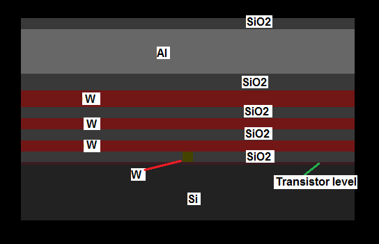 Figure 5. Model in GEANT4 with tungsten metallization and aluminum power line.
In Figure 6 the reaction after neutron radiation is shown. It was found that a lot of reactions occur in the Tungsten interconnects. This corresponds to observations in [17].
Under high temperature exposure coupled with high voltage or current, beside radiation effects migration effects also play an important rule. Depending on the stress conditions electromigration (EM) or stress migration (SM) are the main driving forces for these failures.
In the case of migration in metallization electro- and stress migration are the main failure mechanism. In the case of solder bumps thermomigration can occur as well [18, 19]. Stress migration occurs preferred at locations with high stress gradients, with a high concentration of vacancies or microstructure defects and at locations with active diffusion pathways with a low activation energy [20].
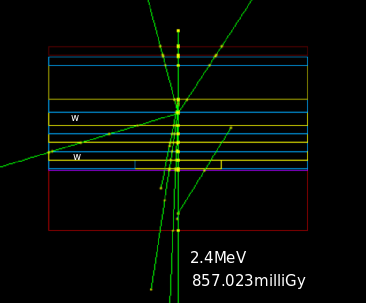 Figure 6. Reaction after neutron radiation with 2.4MeV.
It appears from the literature that the choice of relevant materials is the most discussed issue to enhance device performances as the reduction of interconnect is the “standard” evolution of all systems and cannot be prevented. In particular, the choice of the conducting material has a high influence on the specific resistance, on the homogeneity of thermal gradients, and on hot spots [18].
Migration effects are strong depending on local current densities, heating and stress gradients and the processing temperatures have to be considered [21, 22]. The mass flux describes the strength of the electromigration effect in the metallization structure. The mass flux represents the mass that flows through unit area per unit time. The mass flux of the different mechanisms are given in equation 1-3.
In equation 1-6, j is the local current density, jth the threshold current density N is the number of the activated particles, kB the Boltzmann constant, T the temperature, eZ* the effective charge, ρ the resistivity, D0 the self-diffusion constant, Q* the heat of transport, grad T the temperature gradient, Ω the atomic volume, grad σH the stress gradient and EA the activation energy for the specific mechanism. The resulting divergences are given in equation 4-6.
For divergences bigger than zero a void can occur and for divergences smaller than zero a hillock can grow.
The different material properties for metallization materials as well as SnAgCu (SAC) as solder material are given in table y. It can be seen that the activation energy for tungsten as well as for platinum is higher compared to Al or Cu. The migration process is in the range of x magnitudes smaller compared to aluminum. The use of tungsten helps in this case to decrease migration effects due to the high activation energy for that process.
Table 4. Material properties for the different metallization materials [23-25].
| Material | ρ[µΩcm] | κ[W/mK] | EA[eV] | Z* | Q*[eV] |
| Al | 3.16 | 237 | 0.7 | -10 | -0.104 |
| Cu | 1.74 | 395 | 0.9 | -5.5 | -0.312 |
| W | 5.5 | 174 | 1.7 | 12.4 | 0.009 |
| Pt | 10.5 | 73 | 1.0 | 0.3 | 0.677 |
| SnAgCu | 13.2 | 58.7 | 0.863 | 20 | -0.009 |
2.5. SILVACO TCAD
With SILVACO TCAD the behavior of a transistor after SEU exposure with different energies as well as different LET Doses and a radius of 5nm with a cylindrical way through the transistor were calculated. In Figure 7 the dimensions of the transistor is shown.
The incidence of the SEU began at the drain vertical trough the transistor. The drain current depending on the transient time is shown in Figure 8. The higher the LET dose the sharper the profile of the drain current occurs. Once the onset of the SEU, a prompt charge collection will occur followed by the diffusion charge collection.
Electron-hole pairs with high carrier concentrations are created. If the ionization track traverses or comes close to the depletion region, carriers are rapidly collected by the electric field creating a large current/voltage transient. The ‘prompt’ collections phase follows, indicated in Figure 8. A funnel is created which enhances the efficiency of the drift collection by extending the depletion region deeper into the substrate. The size of the funnel is a function of the substrate doping. This phase is completed within a nanosecond and followed by a phase where diffusion begins to dominate the collection process. Additional charge is collected as electrons diffuse into the depletion region in a time scale of hundreds of nanoseconds until all excess carriers have been collected, recombined, or diffused away from the junction area [26].
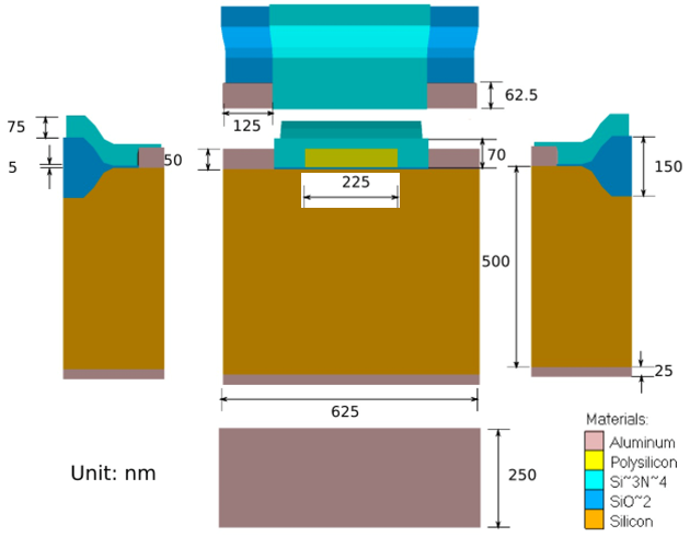 Figure 7. Dimensions of the transistor in SILVACO.
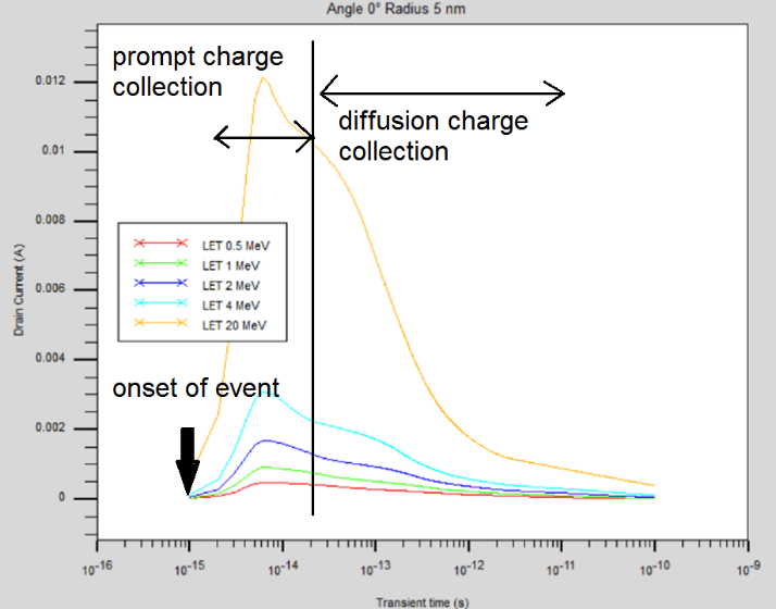 Figure 8. Drain current depending on the transient time for different LET.
2.6. Stacked Dies in 3D-Integration
In 3D integration several memories are stacked one by the other. In Figure 9 a possible scenario of a SEU interaction in 3D integration is shown. This might be an additional problem caused by the fact, that not only one silicon die (die 4) is exposed by alpha emitters from the solder. The die below (die 3) will also be affected due to the strong silicon thinning for stacking the IC’s. Due to the high penetration rate of alpha particles in silicon SEU’s can occur in die 3.
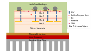 Figure 9. Scheme of stacked dies in 3D integration with possible scenario of SEU interaction.
2.7. SRAM in Different Technology Nodes
After dispensing with boron phosphorus silicate glass (BPSG) in the production processes below the 0.25μm technology node, the proportion of the soft error rate could be reduced by a factor of 10 [27]. From literature it is found that BPSG is also used for technology nodes below 250nm [28]. As a conclusion, it can be seen that thermal neutrons have an influence on the SEU even in small technology nodes. It is well known that commercial of the shelf (COTS) SRAMs were investigated regarding their radiation hardness.
The SRAMs differ concerning the transistor processing in the different technology node of 90nm and 130nm in the gate length as well as the number of the wiring planes. The neutron-induced failure on eight different SRAM components with different neutron energy was investigated and the single event upset (SEU) rate was measured. The test set up and the measurement results are described in [29]. It was found that various sources deal with the analysis of conventional SRAMs of these technology nodes. In [30] SRAMs of the technology nodes 90nm to 350nm are reported. The components were not designated, so that a conclusion regarding manufacturers is not possible. A comparison between the different technologies with respect to their critical charge, shows no linearity between the technology nodes and the critical charge. The consideration of the cell size also shows no linearity with respect to the critical charge. This finding is relevant for the possible establishment of a standard model for checking on the basis of the critical charge.
3. Harsh Condition Effects Mitigation on Programmable COTS Devices
The use of programmable COTS devices in systems for satellites and space missions [31] implies the use of fault tolerant mechanisms at different levels (i.e., system, application, and instruction level) capable of detecting and correcting the previously mentioned (see Section 2.2.) CMOS related failure mechanisms.
In the system level, the duplication or triplication of programmable COTS devices is the most usual technique [32]. Bi-Modular Redundancy (Bi-MR) architectures are mainly used in fail-stop systems, since a duplex mechanism cannot intrinsically correct failures, requiring extra mechanisms that use time redundancy at the application level for diagnostic and recovery. The telemetry module of the Ariane 5 uses a Bi-MR based on COTS digital signal processors [31]. When results on both DSP differ, the results of one DSP are used and the second one is reinitialized. Tri-Modular Redundancy (Tri-MR) architectures also enable the correction of SEUs by reinitializing, for example, this processor which results differ. The Proton100K computer used by Space Micro [33] extended the concept of Tri-MR by applying time redundancy at the application level. The SCS750 space-qualified board [35] implements three IBM PowerPC 750FX working in triplex mode and includes a Radiation Tolerant FPGA, which is in charge of comparing the results among the PowerPC processors. Increasing the number of duplicated modules can increase even more the failure correction rate. For example, the flight control system implemented by Airbus A320/A330/A340 made use of eight computers [34]
In the application level, time redundancy is mostly used consisting in executing two consecutive times the target application on the same processor. Then, the failures are detected when the results of both executions differ. This technique is commonly used in conjunction with Bi-MR or Tri-MR architectures as it is mentioned above.
Replication techniques can also be applied at instruction level. In this case, each instruction is executed twice sequentially on the same processor, followed by a conditional branch. In case the results mismatch, the condition of the following branch instruction is true and the corresponding recovering subroutine is executed. This technique requires a huge memory and can drastically reduce the processing performance. A first software implementation of this technique was presented in [36] and tested on an Intel 8051 microcontroller. In [37], the authors present a new methodology that permits easy combination of hardware and software soft errors mitigation techniques and allows the automatic generation of protected source code, called hardened code.
4. Conclusion
Influences concerning radiation hardness on the components were discussed. The ultra-high integration with new materials and processes influences the SEU risk. For many applications the transition from Pb-free to Sn-based solder materials is done. The risk for alpha emission from the Sn is not eliminated due to the fact that trace contamination of Pb in Sn. Different metallization layers and Tungsten as local interconnect influences the radiation sensitivity. Simulation investigations with tools such as e.g. GEANT4 with a refinement of TCAD simulations e.g. SILVACO can help to understand the radiation impact on the devices. The availability as well as the utilization of such a tool is difficult. BPSG should be history below the 250nm nodes. It is reported, that in 250nm and beyond BPSG is still or again present.
In the case of high temperature and high voltage or current, application migration effects can occur in the metallization or solder material. Migration effects are strong depending on local current densities, heating and stress gradients and the processing temperatures have to be considered by simulation.
Finally examples how to mitigate harsh condition effects on programmable COTS devices are presented on three different design levels.
- Weide-Zaage, K.; Eichin, P.; Chen, C.; et al: COTS – Radiation Effects Appraoches and Considerations, SMTA Pan Pacific Symposium, 2017
- F. Faccio: “COTS for the LHC radiation environment the rules of the game”, [alicedcs.web.cern.ch]
- S. Mitra, P. Sanda, N. Seifert: “Soft Errors: Technology Trends, System Effects and Protection Techniques”, IEEE International On-Line Testing Symposium (IOLTS), 2007.
- Kumar, S; Agarwal, S.; Jung, J.P.: “Soft Error Issue and Importance of low Alpha Solders for Microelectronics Packaging”, Rev. adv. Mater. Sci. 34 (2013) 185-202.
- Baumann, R.C., Smith, E.B., “Neutron-Induced Boron Fission as a Major Source of Soft Errors in Deep Submicron SRAM Devices”, Proc. IEEE International Reliability Physics Symposium, 2000, pp: 152-157.
- Ditali, A.; Hasnain, Z.; “Monitoring alpha particle sources during wafer processing”, Semiconductor International, Vol. 16, No.7, 993, pp: 136-140.
- Levine, S.W.: “Alpha-emission measurements of lids and solder preforms on semiconductor packages”, IEEE Trans. On Comp., Hybrids and Manu. Tech., Vol. CHMT-2, No.4, 1979 pp: 391-395.
- Meieran, E.S.; Engel, P.R; May, T.C.; “Measurement of alpha particle radioactivity in IC device packages”, Proc. IEEE International Reliability Physics Symposium; 1979, pp: 13-22.
- B. M. Clark, D. Grove, T. Unvar: “Alpha radiation Dynamics in Electronics Packaging Structures”, Chip Scale Review, July/August 2013 pp.34-37.
- Reynard, J (2002). “Integration of fluorine-doped silicon oxide in copper pilot line for 0.12-μm technology”. Microelectronic Engineering 60: 113. doi:10.1016/S0167-9317(01)00586-X.
- M. Turowski, A. Raman, G. Jablonski: “Mixed Mode Simulation and Analysis of Digital Single Event Transients in Fast CMOS ICs”, Proc. MIXDES 2007, Ciechocinek, Poland, pp. 433-438.
- C. L. Howe, R. A. Weller, et al, “Role of Heavy-Ion Nuclear Reactions in Determining On-Orbit Single Event Error Rates,” IEEE Trans. Nucl. Sci., vol. 52, Issue 6, part 1, Dec. 2005, pp. 2182-2188.
- S. Kobayashi, D. Ball, et al: “The effect of metallization layers on single event susceptibility,” IEEE Trans. Nucl. Sci., vol. 52, no. 6, pp. 2189–2193, Dec. 2005.
- M. Turowski, A. Fedoseyev, A. Raman: ”Single event upset modeling with nuclear reactions in nanoscale electronics”, Conf. MIXDES, 2008, pp. 443-448.
- M. Raine: “Etude de l’ eff et de l’ energie des ions lourds sur la sensibilite des composants electroniques”, Universite Paris Sud – Paris XI, 2011.
- A. Akkerman, J. Barak: “Ion-Track Structure and its Effects in Small Size Volumes of Silicon”, IEEE Trans. on Nucl. Sci., Vol. 49 No. 6, 2002, pp: 3022-3032.
- H. Zhang, S. Wang, et al: “The effect of heavy metal in CMOS on neutron induced single event upset simulated with Geant4“.
- L. Meinshausen, K. Weide-Zaage, H. Fremont, Electro- and thermo-migration induced failure mechanisms in Package on Package, Microelectronics Reliability 52, pp. 2889-2906, 2012.
- Tu, K. N., Recent Advances on Electromigration in Very-Large-Scale-Integration of Interconnects, Journal of Applied Physics, Vol. 94, no. 9, pp. 5452—5473,, 2005
- E. T. Ogawa, J. W. McPherson, et.al: “Stress-induced voiding under vias connected to wide Cu metal leads”, 2002 Proc. Conf. 40th IEEE (Dallas, TX: IEEE) pp. 312–31.
- K. Weide-Zaage, J. Zhao, J. Ciptokusumo, et.al: “Determination of Migration Effects in Cu-Via Structures with Respect to Process Induced Stress”, Microelectronics Reliability 48, 2008, pp.1393–1397.
- B. L. Park, et al.: “Mechanisms of Stress-Induced Voids in Multi-Level Cu Interconnects,” IEEE 2002 International Interconnect Technology Conference, 2002, pp. 130-132.
- R. C. Weast: “CRC Handbook of Chemistry and Physics”, 62. Edition CRC Press, Boca Raton, Florida 1981.
- H. Weaver: “ Elektro- und Thermotransport in Metallen”, J.A. Barth Leipzig 1973.
- B. Chao, S.-H. Chae, et. al.: “Investigation of diffusion and electromigration parameters for Cu–Sn intermetallic compounds in Pb-free solders using simulated annealing“, Acta Met., 55, 2007, pp.2805-2814.
- R. Baumann: „Radiation-Induced Soft Errors in Advanced Semiconductor Technologies“, IEEE Trans. Dev. Mat. Rel., Bd. 1 Vol. 5, No. 3, 2005.
- Kumar, S; Agarwal, S.; Jung, J.P.: “Soft Error Issue and Importance of low Alpha Solders for Microelectronics Packaging”, Rev. adv. Mater. Sci. 34 (2013) 185-202.
- H. Zhang, H. Jiang. Et al: ”Thermal Neutron-Induced Soft-Error Rates for Flip-flop Designs in 16nm Bulk FinFET Technology”, Proc. IEEE International Reliability Physics Symposium; 2017, 3D-03.
- Zabel, J.; Gudehus, B.; Kaiser, A.; Krüger, K.: Microanalysis of Radiation-sensitive Semiconductors. Annual Military Scientific Research Report 2011, Federal Ministry of Defense, March 2012.
- M. Olmos, R. Gaillard, et al: “Investigation of thermal neutron induced soft error rates in Commercial SRAMS with 0.35µm to 90nm Technology”, IEEE 44th Annual International Reliability Physics Symposium, IRPS, San Jose, 2006.
- M. Pignol. COTS-based applications in space avionics. In Proceedings of the Conference on Design, Automation and Test in Europe (DATE ’10). European Design and Automation Association, 3001 Leuven, Belgium, Belgium, pp.1213-1219, 2010
- M. Pignol, “How to cope with SEU/SET at system level?,” 11th IEEE International On-Line Testing Symposium, 2005, pp. 315-318.
doi: 10.1109/IOLTS.2005.34 - D. Czajkowski, and M. McCartha, Ultra low-power space computer leveraging embedded SEU mitigation. In Proc. IEEE Aerospace Conf (Vol. 5, pp. 2315-2328), 2003
- D. Briere and P. Traverse, “AIRBUS A320/A330/A340 electrical flight controls – A family of fault-tolerant systems,” FTCS-23 The Twenty-Third International Symposium on Fault-Tolerant Computing, Toulouse, France, 1993, pp. 616-623.doi: 10.1109/FTCS.1993.627364
- R. Hillman, G. Swift, P. Layton, M. Conrad, C. Thibodeau and F. Irom, “Space processor radiation mitigation and validation techniques for an 1,800 MIPS processor board,” Proceedings of the 7th European Conference on Radiation and Its Effects on Components and Systems, 2003. RADECS 2003., Noordwijk, The Netherlands, 2003, pp. 347-352.
- M. Rebaudengo, M. S. Reorda and M. Violante, “A new software-based technique for low-cost fault-tolerant application,” Annual Reliability and Maintainability Symposium, 2003., 2003, pp. 25-28. doi: 10.1109/RAMS.2003.1181897
- A. Martinez-Alvarez, S. Cuenca-Asensi, F. Restrepo-Calle, F. R. Palomo Pinto, H. Guzman-Miranda and M. A. Aguirre, “Compiler-Directed Soft Error Mitigation for Embedded Systems,” in IEEE Transactions on Dependable and Secure Computing, vol. 9, no. 2, pp. 159-172, March-April 2012. doi: 10.1109/TDSC.2011.54