Optimal Synthesis of Universal Space Vector Digital Algorithm for Matrix Converters
Optimal Synthesis of Universal Space Vector Digital Algorithm for Matrix Converters
Volume 2, Issue 3, Page No 147-152, 2017
Author’s Name: Adrian Popovicia), Mircea Băbăiţă1, Petru Papazian2
View Affiliations
Applied Electronics Department, Politehnica University Timisoara, 300223, Romania
a)Author to whom correspondence should be addressed. E-mail: adrian.popovici@upt.ro
Adv. Sci. Technol. Eng. Syst. J. 2(3), 147-152 (2017); ![]() DOI: 10.25046/aj020319
DOI: 10.25046/aj020319
Keywords: Space vector, Digital algorithm, Modulation, Matrix converter, Transfer function, Switching function

Export Citations
This paper presents the synthesis of a dynamic space vector modulation for power matrix converters so that it is possible to implement a universal modulator that provides a control algorithm dynamically optimized according to the requirements for the matrix converter.
Received: 04 March 2017, Accepted: 07 April 2017, Published Online: 20 April 2017
1. Introduction
In recent years the three-phase to three-phase matrix converter has received considerable attention as an alternative to hard and soft switching dc link converters. This paper is an extension of work originally presented in International Symposium on Electronics and Telecommunications ISETC ‘16 Twelfth Edition [1]. The SVM (space vector modulation) control strategy for matrix converter offers the best performance, maximal voltage gain and controllable input displacement factor. There are several possible SVM algorithms focused first on reducing energy losses or optimizing the parameters for output voltage and input current [2]. The optimum choice of one of the SVM techniques is a complex task because these requirements are contradictory since reduced power losses mean a reduced sampling frequency leading to a degree of large distortion of waveforms generated by the matrix converter. So for choose correctly a control technique it is required a prior accurate knowledge of the specific conditions which the matrix converter will operate and the characteristics of semiconductor devices which implement the bidirectional switches [3]. Therefore, depending by the operation mode of the power circuit and the conditions imposed by the nature of the load it is useful an implementation of an universal algorithm enabling the transition from an reducing energy losses mode to a very low distortion of the generated waveforms mode and possibility to operation intermediate regimes between them. For this reason it is necessary to implement a digital modulator circuit that allows switching from one SVM algorithm to another without major modifications of the hardware control circuit.
2. Space Vector Modulation
The matrix converter consists of nine bidirectional switches that connect the three outputs with each of the three inputs, as shown in Figure 1. The converter being supplied by a voltage source, the three input phases can’t be short-circuited, and the load having generally a mainly inductive character, the load current can’t be interrupted. Because of these constraints the nine switches can generate only 27 permitted combinations. The SVM control algorithm uses 21 of these combinations, a number of 18 combinations, A122- A133; B212-B313 and C221-C331 which connect two output phases at the same input, called active states and a number of 3 combinations Z111-Z333 with all three outputs connected at the same input, called passive states of the matrix converter. To analyze the SVM modulation applied to a three-phase system x1, x2, x3, the space vector X of the system can be used, represented in the complex plan according to the transformation:
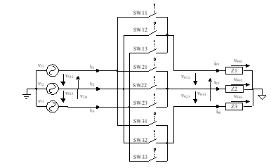
Figure 1: The matrix converter switch layout
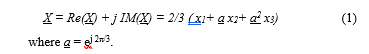
According to this transformation the desired output line voltages space vector is V0LW which rotates with the w0 angular speed, and the desired input phase currents space vector is IIW which rotates with wI angular speed as shown in Figure 2 and Figure 3 respectively.
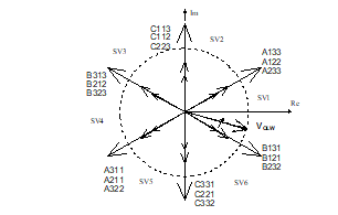
Figure 2: Output voltage SVM vectors diagram
Figure 3: Input current SVM vectors diagram
The circular trajectories of these vectors can be divided in six voltage and current sectors, SV and SC respectively. If Ts time interval is short enough so that the reference vectors VOLW and IIW do not change significantly, the mean vector space result from different combinations of stationary space vector and null corresponding input voltage line will be equal with the reference vector in this time. Simultaneously it must be performed the desired phase difference between the input current reference space vector and the input voltage space vector, through various combinations of stationary and null space vector corresponding to input currents. The best approximation of spatial reference vector at a time, can be done using vectors that have direction adjacent with the reference space vector [2]. The principle is shown in Figure 4a and Figure 4b, where a,b and m,n are adjacent directions for output voltage reference space vector and input current reference space vector, respectively. In Figure 4c and Figure 4d it is shown how to choose the vectors for SV1 and SC1 active sectors. In this way from the 21 matrix converter permitted states, in any moment only four active states uniquely established and one of the passive states can simultaneously synthesise the two reference vectors [4]. The order of these active states and the passive state required in a sampling period are chosen so that the number of switches is minimum. Using the trigonometric laws, the normalised time intervals in a sampling period Ts, corresponding
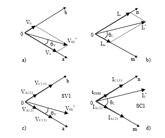
Figure 4: The space vector modulation principle
to the four active states can be established: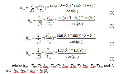
For example, the relation between output and input voltages is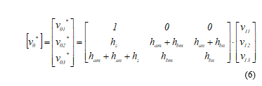
for SV1 and SC1 active sectors. This fact means that the normalised time intervals ham, han, hbm, hbn, hz represent the transfer functions for the SVM control strategy.
3. SVM1-SVM3 Versions of Space Vector Modulation
For a three-phase voltage supply for a given three phase output voltages and input phase shift between current and voltage, the association between active SVM and permitted matrix converter states is unique (Table 1). If you know the TS, then periods Tam, Tbm, Tan, Tbn, can be calculated with relationships (2)-(5). In the time interval Tz the matrix converter can pass in any of the passive states. The order in which matrix converter switches from one state to another, within the time Ts, does not affect the local average value of voltages and currents [2],[5]. Basically, choosing between passive states and the order in which the converter switches from one state to another, does not affect the fundamental components of generated waveforms, but it determines the number of commutations required per unit time and the spectral characteristics of generated waveforms. Generally it is intended that the arrangement of the matrix converter states matrix in a sampling period TS is made such that are necessary as few commutations when passing from one state to another. For example if the active sectors are SV1 and SC1 respectively, then from Table 1, the correlation between active states and switching states is am, bm, an, bn and A121, A122, C131, C133 respectively. If a sampling period will use the SVM sequence am – bm – bn – an -z , then this corresponds to sequence A121 -(1)- A122 -(1)- C133 -(2)- C131 -(1)- Z111-(1)-…, if the z state is associated with Z111state. It is noted that in this case 6 switching are required within the sampling period TS. If it is kept the same SVM sequence and combination of active sectors is SV1-SC2 then the sequence becomes C131 -(1)- C133 -(1)- B233 -(1)- B232 -(3)- Z111-(1)-… which means that required 7switching/TS. But if the SVM combination is changed as follows bm – am – an – bn -z , then we have the next switching sequence: C133 -(1)- C131 -(2)- B232 -(1)- B233 -(1)- Z333-(1)-…, if zero state is associated with Z333 state. It is noted that in this case it is required 6switching/TS too. Generalizing for all possible combinations it is obtained the Table 2 association which can be easily implemented in a digital control system. Depending on the combination of the active sectors at a time, we define the complementary logical variables Pa and Pb, as follows: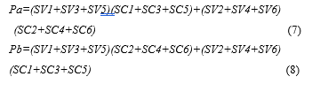
Table 1: Matrix converter active states and SV, SC sectors association
|
Voltage Sector SV |
Current Sector SC | Active State am |
Active State bm |
Active State an |
Active State bn |
|
1 1 1 1 1 1 |
1 2 3 4 5 6 |
A121 C131 B232 A212 C313 B323 |
A122 C133 B233 A211 C311 B322 |
C131 B232 A212 C313 B323 A121 |
C133 B233 A211 C311 B322 A122 |
|
2 2 2 2 2 2 |
1 2 3 4 5 6 |
A122 C133 B233 A211 C311 B322 |
A112 C113 B223 A221 C331 B332 |
C133 B233 A211 C311 B322 A122 |
C113 B223 A221 C331 B332 A112 |
|
3 3 3 3 3 3 |
1 2 3 4 5 6 |
A112 C113 B223 A221 C331 B332 |
A212 C313 B323 A121 C131 B232 |
C113 B223 A221 C331 B332 A112 |
C313 B323 A121 C131 B232 A212 |
|
4 4 4 4 4 4 |
1 2 3 4 5 6 |
A212 C313 B323 A121 C131 B232 |
A211 C311 B322 A122 C133 B233 |
C313 B323 A121 C131 B232 A212 |
C311 B322 A122 C133 B233 A211 |
|
5 5 5 5 5 5 |
1 2 3 4 5 6 |
A211 C311 B322 A122 C133 B233 |
A221 C331 B332 A112 C113 B223 |
C311 B322 A122 C133 B233 A211 |
C331 B332 A112 C113 B223 A221 |
|
6 6 6 6 6 6 |
1 2 3 4 5 6 |
A221 C331 B332 A112 C113 B223 |
A121 C131 B232 A212 C313 B323 |
C331 B332 A112 C113 B223 A221 |
C131 B232 A212 C313 B323 A121 |
Table2: Sequence SVM states and voltage current sectors association for 6switchings/TS
| Active Sectors | SVM States Sequence |
|
SV1-SC1 SV1-SC3 SV1-SC5 SV2-SC2 SV2-SC4 SV2-SC6 SV3-SC1 SV3-SC3 SV3-SC5 SV4-SC2 SV4-SC4 SV4-SC6 SV5-SC1 SV5-SC3 SV5-SC5 SV6-SC2 SV6-SC4 SV6-SC6 |
am – bm – bn – an -z |
|
SV1-SC2 SV1-SC4 SV1-SC6 SV2-SC1 SV2-SC3 SV2-SC5 SV3-SC2 SV3-SC4 SV3-SC6 SV4-SC1 SV4-SC3 SV4-SC5 SV5-SC2 SV5-SC4 SV5-SC6 SV6-SC1 SV6-SC3 SV6-SC5 |
bm – am – an – bn -z |
This SVM version can be changed if the passive state z is placed at the beginning of the sampling period z- am- bm- bn -an for Pa =1 and z- bm- am- an- bn for Pa =0 or z- an- bn- bm- am and z- bn- an- am- bm for Pa=1 and Pa=0, respectively. The combination of the SVM sequences and the matrix converter states can be easily implemented by some memory circuits. The variant thus obtained will be referred to as SVM1. This principle is shown in Figure 5 for a sampling period. Again 6 switchings/TS are necessary if for Pa =1 the SVM sequence is an- bn- bm- am – z and for Pa =0 it is bn- an- am- bm- z . Tis s SVM1a algorithm. The SVM1 version can be modified if the zero state is at the
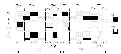
Figure 5: Line output voltage generation in the sampling period for SVM1 algorithm
beginning of the sequence z- am – bm –bn – an for Pa=1 and z- bm – am – an – bn. for Pa=0. This is SVM1b algorithm.
By modifying the SVM1 algorithm in the same way we can get the algorithm SVM1c ie z- an – bn –bm – am for Pa=1 and z- bn – an – am – bm. for Pa=0. Again 6 switchings/TS are necessary if the passive state is placed between active states: bm- am- z- an- bn and am- bm- z- bn- an for Pa =1 and Pa =0 or bn- an- z- am- bm and an- bn- z- bm- am for Pa =1 and Pa =0 synthesizing another algorithms named SVM1d and SVM1e respectively. A further reduction in the number of commutations can be made by combining certain type of previous algorithms. These new combinations will be named SVM2. A first additional reduction in the number of commutations can be done if for three consecutive sampling periods the SVM sequences will be SVM1b – SVM1e – SVM1 or SVM1c – SVM1d – SVM1a, versions thus obtained are called SVM2a and SVM2b. For example, for SVM2a and SC1-SV1 active sectors the SVM sequence will be z- am- bm- bn- an- bn- an- z- am-bm- am- bm- bn- an- z for Pa =1, which means that the number of commutation will be reduced with 5.5%. It can also be reduced the number of switching whether to combine two types of SVM1 sequences for two consecutive sampling periods in sequences SVM1-SVM1c, SVM1a-SVM1b and SVM1d-SVM1e, synthesizing the control techniques SVM2c, SVM2d and SVM2e, respectively. For example for SVM2c and SV1-SC1 active sectors, if Pa =1 the matrix converter sates will be A121-(1)-A122-(2)-C133-(1)-C131-(1)-Z111-(0)-Z111-(1)-C131-(1)-C133 -(2)-A122-(1)-A121-(0)- therefore it means that two consecutive sampling periods requires 10 switching so that the average switching requires 5switchings/TS. This means a 16% reduction in the necessary number of commutations.
Another direction is optimization techniques to control the dominant harmonics, movement of these to high frequencies, for the same sampling frequency, without increasing excessive the switching losses. This can be achieving using symmetrical waveforms to the center of the sampling period [3]. Variants proposed in the literature accomplishes this balancing around the passive state, which is placed in the center of the sampling period, being framed by the active states that are divided into equal time intervals placed at the beginning and the end of the sampling period. To minimize the number of necessary switching sequences the implementation of SVM sequences proposed in this paper are am/2- bm/2- bn/2- an/2- z- an/2- bn/2- bm/2- am/2 for Pa =0 and bm/2- am/2- an/2- bn/2- z- bn/2- an/2- am/2- bm/2 for Pa=1. This version is named SVM3. For this type of algorithms, the converter switches between 9 states during a sampling period, so the minimum number of commutations required is 8switching/TS. If the SVM sequences are an/2- bn/2- bm/2- am/2- z- am/2- bm/2- bn/2- an/2 for Pa =0 and bn/2- an/2- am/2- bm/2- z- bm/2- am/2- an/2- bn/2 for Pa =1 then are necessary 8switching/TS too. This is named SVM3a algorithm. For SVM3 the output voltage is symmetrical around “big” pulses, while for SVM3a it is symmetrical around “low” pulses for angle qC=0-30° in each current sector and vice versa for qC =30-60°. În [4] it is suggested that maintaining symmetry around the “big” or “small” voltage pulses regardless of the angle qC this can improve the quality of spectral waveforms generated at the converter output matrix. If for qC =0-30° will be used SVM3a and for qC =30-60° will be used SVM3, then at any time the output voltage waveform will have a shape symmetrical around “small” voltage pulses. This is SVM3b technique. If it is used SVM3 for qC =0-30° and SVM3a for qC =30-60°we will have symmetry around „large” pulses. This is SVM3c. An improvement of the quality of the frequency spectrum for the waveforms generated by the matrix converter can be obtained by alternating “big” voltage pulses with “small” voltage pulses keeping the symmetry of the output voltages [4]. In order to implement this technique it is necessary to control all switchings between nine states that requires 10 switching/TS which results in an increase of 66% in the number of switching per unit time. To implement this technique it is necessary to control all switching between nine states. But if in a sampling period is chosen the sequence bn/2- an/2- z/2- am/2- bm- am/2- z/2- an/2- bn/2 for Pa =1 and an/2- bn/2- z/2- bm/2- am- bm/2- z/2- bn/2- an/2 for Pa =0 or bm/2- am/2- z/2- an/2- bn- an/2- z/2- am/2- bm/2 and am/2- bm/2- z/2- bn/2- an- bn/2- z/2- bm/2- am/2, for Pa =1 and Pa =0 respectively then it is possible to reduce the number of commutation to 8commutations/TS. This is SVM3d algorithm. If the sequences are z/2-bn/2- an/2- am/2- bm- am/2- an/2- bn/2- z/2 for Pa=1 and z/2-an/2- bn/2- bm/2- am- bm/2- bn/2- an/2- z/2 for Pa=0 then we obtain version SVM3e. For
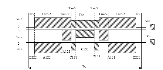
Figure 6: Line output voltage generation in the sampling period for SVM3d algorithm
angle qC=0-30°, SVM3d generates symmetrical waveforms around the „small” voltage pulses like in Figure 6 and SVM3e around “big” voltage pulses, and qC =30-60° we have a reversed situation. If for qC=0-30° we will use SVM3e and for qC =30-60° we will use SVM3d, then at any time the output voltage waveform will be symmetrical around “high” pulses and the algorithm will be named SVM3f. If for qC=0-30° we will use SVM3d and for qC =30-60° we will use SVM3e, then at any time the output voltage waveform will be symmetrical around “small” pulses and the algorithm will be named SVM3g. If in a sampling period it is chosen the sequence bn/2- an/2- z/2- am/2- bm- am/2- z/2- an/2- bn/2 for Pa =1 and an/2- bn/2- z/2- bm/2- am- bm/2- z/2- bn/2- an/2 for Pa =0 we will obtain SVM3h. If for Pa =1 and Pa =0 we will have bm/2- am/2- z/2- an/2- bn- an/2- z/2- am/2- bm/2 and am/2- bm/2- z/2- bn/2- an- bn/2- z/2- bm/2- am/2 respectively then we will obtain SVM3i. These algorithms are characterized by 8 switchings/TS too, the waveforms being symmetrically around the center of tha sampling period. The output voltages consist of alternative “high” and “small” voltage pulses set apart by intervals of “zero” voltage. Combining SVM3i and SVM3h in the same manner we will be obtain SVM3i and SVM3k characterized by waveform that are symmetrical around only the “high” pulses or only around the “small” voltage pulses. A detailed analyses of these algorithms will be presented in a future paper.
4. Implementation of the SVM1-SVM3 Modulator
Whichever you choose to control SVM algorithm, a computer system will determine the value of transfer functions ham, han, hbm, hbn şi hz, at TS time intervals. These transfer functions are then transformed into S11-S33 switching functions, which controls the ON/OFF states of the 9 bidirectional switches. To convert these transfer functions in PWM switching functions are sufficient four timers TM1-TM4. For this calculus it is necessary to know the modulation index m=V0L/V0L max or V0/V0 max, space vector angles qC şi qV and input phase angle. Analyzing the proposed variants of SVM algorithm previous proposed it is noted that according to the sequence of matrix converter switching states are 12 possible combinations of timer intervals TM1-TM4, according to the timeframes Tam=ham×TS, Tbm= hbm×TS , Tan= han×TS , Tbn= hbn×TS and Tz=hz×TS. These combinations, denoted CTV1-CTV12 are presented in Table 3. For example for CTV1 combination the logical signals ST1-ST4 at the outputs of timers will be like in Figure7. The switching functions S11-S33 associated with switches of the matrix converter are calculated based on the combinations of CTV, SV, SC variables and auxiliary variables Pam, Pbm, Pbn, Pan and Pz calculated based on the five possible states of the signals ST1-ST4. For example switching function formula for S11 is given by equation (9).
S11 = Pam (( SC1+ SC2) ( SV1+ SV2+ SV3)+( SC4+ SC5) (SV4+ SV5+ SV6))+Pbm (( SC1+ SC2) ( SV1+ SV2+ SV6)+( SC4+ SC5) (SV3+ SV4+ SV5))+Pbn (( SC1+ SC6) ( SV1+ SV2+ SV6)+(SC3+ SC4) ( SV3+ SV4+ SV5))+Pan (( SC1+ SC6) (SV1+ SV2+ SV3)+(SC3+ SC4) ( SV4+ SV5+ SV6))+Pz (Saz1× ( SC1+ SC4) + Saz2 × ( SC3+ SC6) + Saz3 × ( SC2+ SC5)) (9)
Formula (10) is an example calculation for auxiliary variable Pam
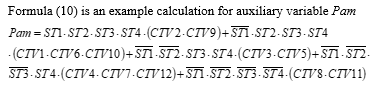 (10)
(10)
Saz1-Saz3 variables are associated with the passive states z of the converter.
Table 3: The time intervals generated by timers
| TM1 | TM2 | TM3 | TM4 | |
| CTV1 | Tbm | Tbm+ Tam | Tbm+ Tam+ Tan | Tbm+ Tam+ Tan+ Tbn |
| CTV2 | Tam | Tam+ Tbm | Tam+ Tbm+ Tbn | Tam+ Tbm+ Tbn+ Tan |
| CTV3 | Tbn | Tbn+ Tan | Tbn+ Tan+ Tam | Tbn+ Tan+ Tam+ Tbm |
| CTV4 | Tan | Tan+ Tbn | Tan+ Tbn+ Tbm | Tan+ Tbn+ Tbm+ Tam |
| CTV5 | Tz | Tz+ Tbm | Tz+ Tbm+ Tam | Tz+ Tbm+ Tam+ Tan |
| CTV6 | Tz | Tz+ Tam | Tz+ Tam+ Tbm | Tz+ Tam+ Tbm+ Tbn |
| CTV7 | Tz | Tz+ Tbn | Tz+ Tbn+ Tan | Tz+ Tbn+ Tan+ Tam |
| CTV8 | Tz | Tz+ Tan | Tz+ Tan+ Tbn | Tz+ Tan+ Tbn+ Tbm |
| CTV9 | Tam | Tam+ Tbm | Tam+ Tbm+ Tz | Tam+ Tbm+ Tz+ Tbn |
| CTV10 | Tbm | Tbm+ Tam | Tbm+ Tam+ Tz | Tbm+ Tam+ Tz+ Tan |
| CTV11 | Tan | Tan+ Tbn | Tan+ Tbn+ Tz | Tan+ Tbn+ Tz+ Tbm |
| CTV12 | Tbn | Tbn+ Tan | Tbn+ Tan+ Tz | Tbn+ Tan+ Tz+ Tam |
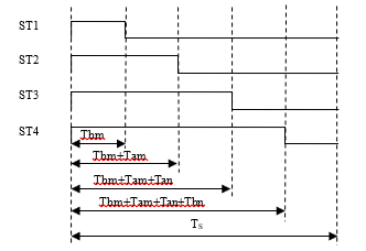
Figure 7: The logical signals at the timers output
The output voltage waveforms and the frequency spectrum for
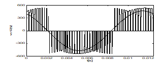
Figure: 8. Output line voltage waveform for SVM1 algorithm
SVM1 algorithm using S11-S33 switching functions generated with the universal modulator are presented in Figure 8, Figure 9
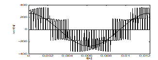
Figure 9: Output phase voltage waveform for SVM1 algorithm
and Figure 10.
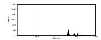
Figure 10: Frequency spectrum of phase output voltage for SVM1
5. Conclusion
In this paper it was presented a dynamic algorithm that enables the implementation of a universal SVM1-SVM3 modulator to control the matrix converters. In this way it is possible to choose different control options that are optimized for reducing energy losses or to control the dominant harmonics. A more detail comparative analysis of these algorithms will be presented in a future work.
Conflict of Interest
The authors declare no conflict of interest.
- Popovici, M. Babaita, P. Papazian “Synthesis of Universal Space Vector Modulator for Matrix Converters”, 2016 12th International Symposium on Electronics and Telecommunications (ISETC) October 27-28, Timisoara, pp. 211-214, 2016.
- L. Huber, D. Borojevic, “Space vector modulated three-phase to three-phase matrix converter with input power factor correction”, IEEE Tran. Ind. Appl., vol.31, no.6, pp. 1234-1246, 1995.
- B.K. Bose, “Power Electronics and Variable Frequency Drives – Technology and Applications”, IEEE, New York, 1997.
- A. Popovici, “Contributii la cercetarea si dezvoltarea convertoarelor matriceale de curent alternativ”, Ph.D Thesis, Politehnica University Timisoara, 2002.
- S. M. Dabour E.M. Rashad, “Analysis and implementation of space-vector-modulated three-phase matrix converter”, IET Power Electronics Journal, Volume 5, Issue 8, pp.1374–1378, September 2012.
- A. Popovici, V. Popescu , Simulation and Implementation of Control Strategy for Matrix Converters Using Simulink Software Package, European Power Electronics And Drives Association-PEMC 2004 Riga, Latvia.
- A. Popovici, V. Popescu, Simulation and Analyses of Matrix converter circuits, European Power Electronics and Drives Association-PEMC 2004 Riga, Latvia.
- A. Popovici, V. Popescu, M. Băbăiţă, D. Lascu, D. Negoiţescu, The Analysis Of Input Filter For Matrix Converters, WSEAS Transactions on Signal Processing, Issue 2, Volume 2, ISSN: 1790-5022, pp. 182-189, February 2006.
- P. Nielsen, F. Blaabjerg, J. Pedersen; Space vector modulated matrix converter with minimised number of switchings and a feedforward compensation of input voltage unbalance; PEDES’96, vol.2, pg. 833-839; 1996.
- A. Popovici, V. Popescu, M. Băbăiţă, D. Lascu, D. Negoiţescu, Modeling, Simulation and Design of Input Filter for Matrix Converters, WSEAS International Conference on Dynamical Systems and Control, Venice, Italy, ISBN: 960-8457-37-8, pp 439-444, November 2-4, 2005.