Stability and nonlinear controller design of Fast-Lock Phase-Locked Loop in 0.18-µm CMOS
Stability and nonlinear controller design of Fast-Lock Phase-Locked Loop in 0.18-µm CMOS
Volume 2, Issue 3, Page No 1266-1271, 2017
Author’s Name: Fatima Al-Mutairi1, a), Reem Al-Mutairi2
View Affiliations
1Department of Electrical and Computer Engineering, Texas A & M University, 77843, College Station, TX
2Department of Electrical Engineering, Kuwait University, 965, Kuwait
a)Author to whom correspondence should be addressed. E-mail: falmutairi@tamu.edu
Adv. Sci. Technol. Eng. Syst. J. 2(3), 1266-1271 (2017); ![]() DOI: 10.25046/aj0203160
DOI: 10.25046/aj0203160
Keywords: Adaptive controller, Stability, Phase Margin(PM), Frequency divider, VCO, PLL

Export Citations
This paper introduces a kind of novel backstepping phase- locked loops (PLL). The paper presents a developed theoretical model of (PLL) frequency synthesizer and provides analytical equations for calculating the desired specification such as phase margin (PM). The proposed model aims to improve the control accuracy, ensure stability and reducing the lock time. Adaptive controller algorithm has been used to design a conventional phase locked loop to operate at 2.2GHz using 0.18µm CMOS technology. The lock time was reduced by adding nonlinear controller in addition with the low-pass filter (LPF) and the tuning variables of the adaptive control to ensure the control accuracy. The simulation results confirm that the stability of the system has been improved and increase Phase Margin (PM) from 56o to 60o. Furthermore, the simulation results indicate that the performance of adaptive PLL control has greater speed response and smaller overshoot than conventional PLL. The lock time for the conventional PLL was 2.1 µs and it is reduced to 1 µs by adding adaptive controller, showing a reduction of the lock time by 53% over the classical PLL.
Received: 01 June 2017, Accepted: 13 July 2017, Published Online: 28 July 2017
1. Introduction
Modeling PLLThis paper is an extension of work originally presented in conference [1]. The phase-locked loop (PLL) considered as an important part in many applications. Phase-Locked loop (PLL) has been widely used in different applications such as electronic application, communication system etc. [2]. Moreover, it is used for data transmission and are manufactured as integrated circuit [3]. PLL considered as an electronic circuit with voltage driven oscillator that permanently adjust to correspond the frequency of an input signal. PLL has been used to generate, stabilize, filter or recover signal from noisy communication channel [4]. Most application of different system requires the oscillator to be tunable [5]. Therefore, their output frequency will be a function of a control input and frequency can be adjusted or controlled by voltage of the control signal. Stability of the system is a critical issue for many designers. Phase margin consider as one of the stability metrics for assigning system robustness. This paper includes stability analysis of the PLL to remain system unchanged over time from external condition.
The systematic model of the phase- locked loop (PLL) nonlinear controlled system is shown in Figure 1. Moreover, the linearized model of the PLL and nonlinear controller is illustrated in Figure 2. The PLL consists of the voltage control oscillator, phase frequency detector, charge pump, divider and traditional low-pass filter. The first functional block of the PLL is the PFD (phase frequency detector) which effects on the performance of the PLL where it compares the phase of two input signal one usually comes from VCO [5]. Figure 3 and Figure 4 show the structure of PFD. Secondly, the charge pump works as a switch current source that controlled by the phase difference between oscillator and reference [6]. Figure 5 shows the charge pump. Furthermore, the loop filter and backstepping controller are considered as a one of functional block of PLL. The second order loop filter is shown in Figure 6. The voltage gains of the VCO (voltage-controlled oscillator) is a major parameter in the PLL that effects lock time [7]. An illustration of the three stages current-starved VCO (CS-VCO) is shown in Figure 7. Frequency divider consists of TSPC technique. TSPC employs a true single-phase clock that is the only clock signal needed and never inverted, which avoids the usage of two non-overlapping two-phase clocks and thus increase the speed [8]. The divider based on TSPC is shown in Figure 8.
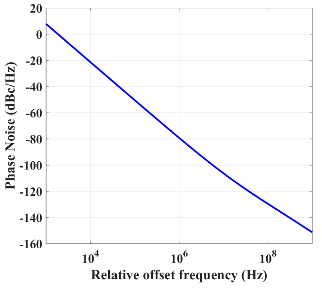
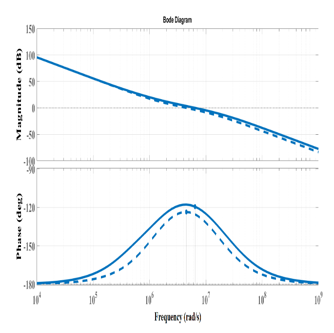 Figure 1: Systematic model of Phase Locked Loop with adaptive Control

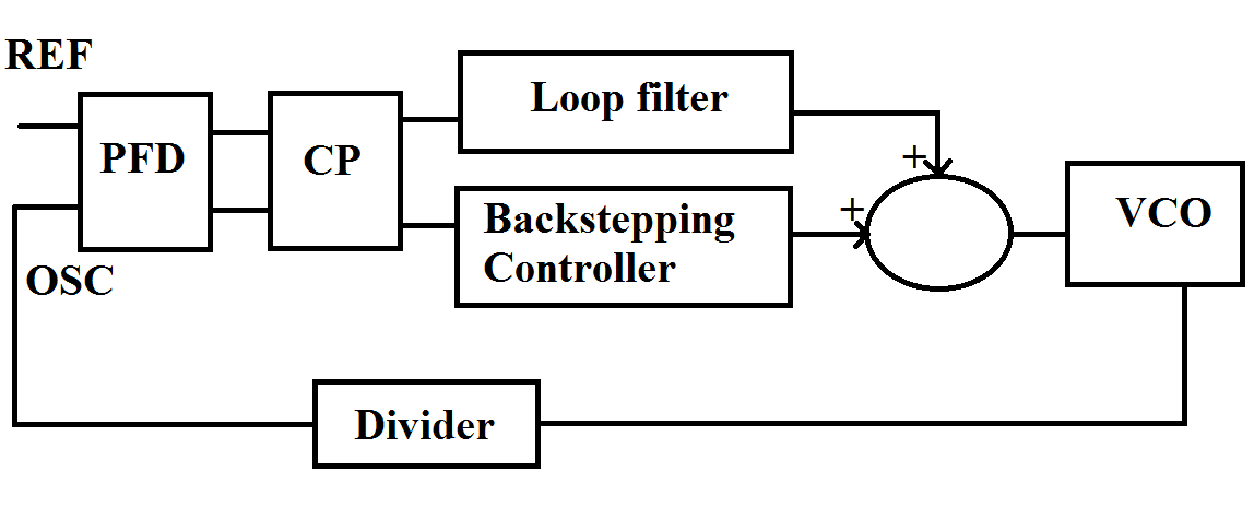
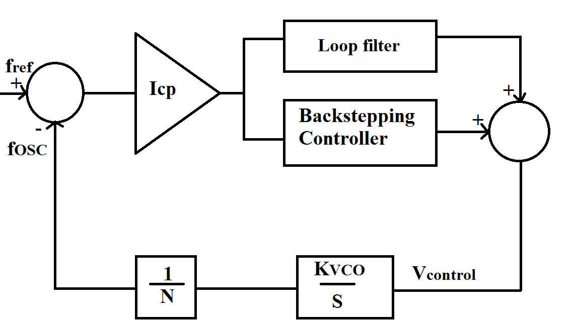
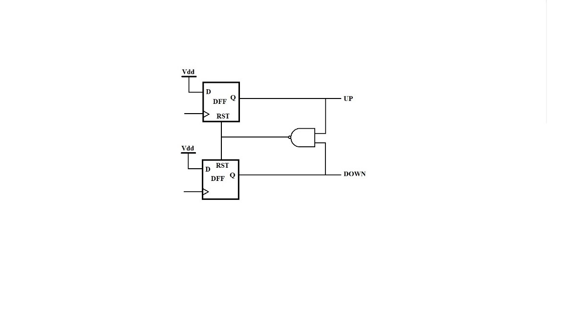
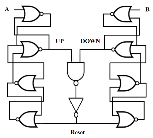
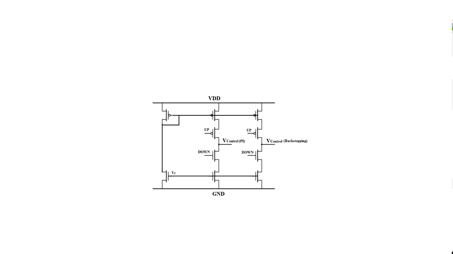
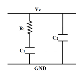
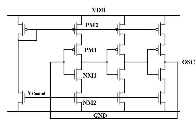

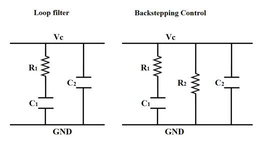
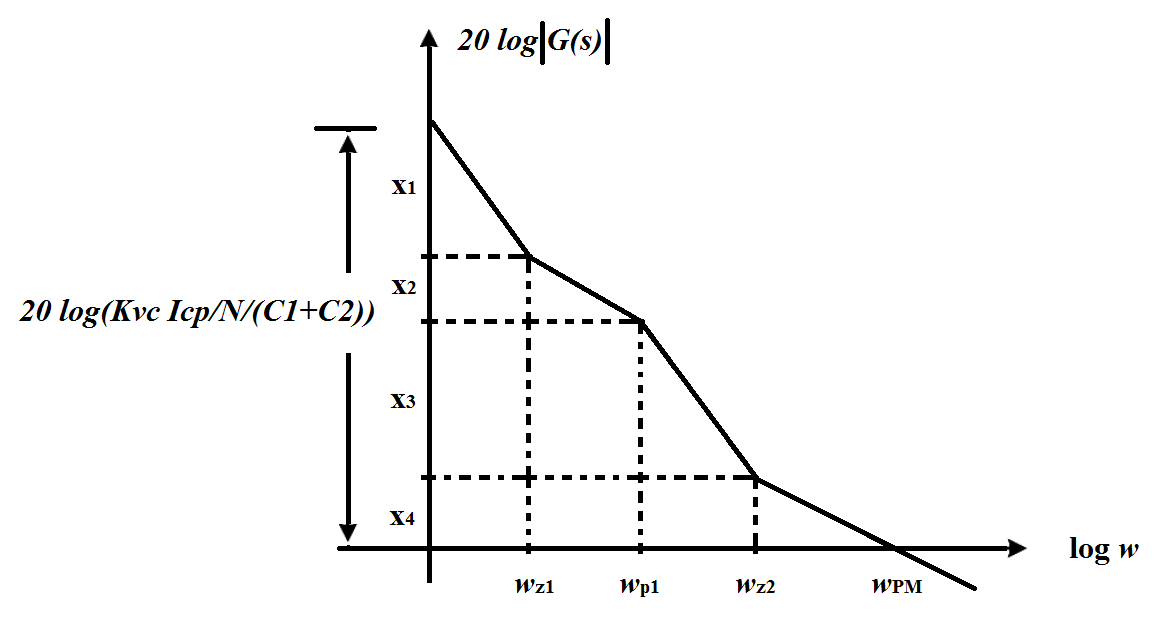
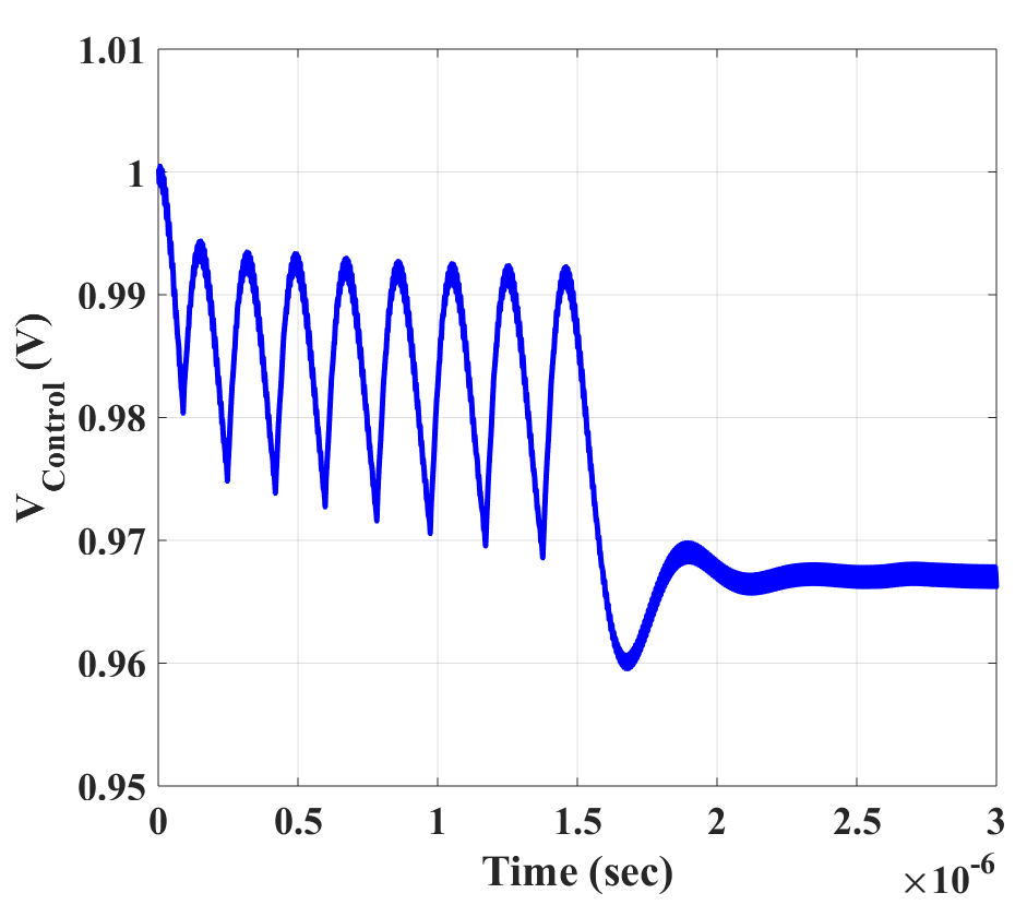
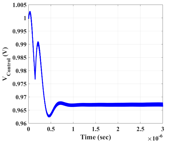
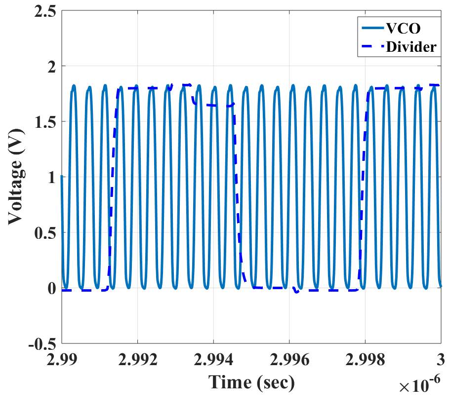
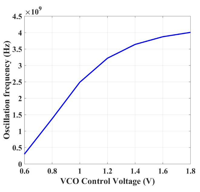 Figure 2: Linearized model of the system
Figure 3: PFD
Figure 4: Structure of the PFD
Figure 5: Structure of the CP
Figure 6: Loop Filter
Figure 7: Structure of the current-Starved VCO
Figure 8: Structure of the TSP
3. Theoretical Analysis
Backstepping design technique is a motivating topic for many researchers, it is widely used and became as one of the featuring new methods for stabilizing strict-feedback, nonlinear systems [9]. Backstepping control is a nonlinear control that used one of the state as a control input to control the other states [10]. The technique is based on generating a family of global asymptotically stabilizing control laws starting the design procedure by defining stable system and determining controller that gradually stabilize each outer subsystem. The process terminated when the external control is attained [11]. The method basically depends on applying Lyapunov functions in which guarantees the stability of the related system [12].
4. Design Proposed
In this section, we will explain the steps needed to implement the backstepping method. The open loop transfer function of PLL can be defined in Equation (1).
is the VCO gain and Icp is the charge pump current. Finding the state space of the system from the transfer function Equation (1).
Rearrangement the system is the first procedure of the backstepping controller.
The schematic of backstepping controller is shown in Figure 9.
Figure 9: Backstepping Control
5. Stability Analysis
The open loop transfer function of PLL system is shown in equation (12).
The magnitude of the G(s) has been plotted with respect to frequency ω as shown in Figure 10.
Figure 10: Bode Plot of the G(s)
The crossover frequency ( ) has been determined [13].
The phase margin can be calculated as shown below:
6. System Simulation
A 0.18µm CMOS technology was used to simulate the proposed design, test and verify the dynamic response of backstepping phase lock loop (PLL). The transistors size of the VCO, Divider, Gates and Charge Pump is shown in Table 1. Maximum overshoot and settling time have been considered as a performance metrics to compare the performance of conventional PLL and backstepping controller with PLL. The comparison between the actual PLL and the implementation of backstepping controller with PLL has been shown in Figure 11 and Figure 12 respectively. The results based on proposed design is showing a smaller overshoot and fast response time with lock time of 1µs where the lock time of the classical PLL was 2.1µs. The new scheme increases the speed and make the system more faster in order to settle the desired voltage where each voltage applying to the VCO represents as a frequency as shown in Figure 12. Figure13 shows Division ratio. The division ratio is 16 when the input and output frequencies are 2.3 GHz and 142 MHz. Figure 14 shows the increased of the measured tuning range of the VCO. The measured tuning range increases from 0.3 to 4 GHz, as the control voltage is increased from 0.6 to 1.8 V. Figure 15 represents that the phase noise is -79.24 dBc/Hz at 1MHz offset. The performance summary of this paper is shown in Table 2.
Figure 11: Transient response of the Conventional PLL
Figure 12: Transient response of the PLL with Backstepping
Figure 13: Transient response of the divider
Figure 14: Tuning range of the VCO
Figure 15: Phase noise of VCO
To insure stability, the phase margin should be at least 45 degree. Typically, the value of C2/C1 is set in the range of 1/10 to 1/6 for conventional PLL that limit phase margin and settling time. By adding backstepping the phase margin is function of R2 and it is improved as shown Figure 16 and Figure 17. The phase margin without backstepping is 56.4˚ and with backstepping is 60.6˚.The improvement is 7.44%.
Figure 16: Bode plot of open loop
Table 1: Sizing of the Transistors
| Device | Transistor | Ratio |
| VCO | PM1 | 27.778 |
| PM2 | 28.333 | |
| NM1 | 11.667 | |
| NM2 | 11.111 | |
| Divider | PM | 16.667 |
| NM | 11.111 | |
|
Not Gate |
PM | 27.78 |
| NM | 11.67 | |
|
Nand Gate |
PM | 27.78 |
| NM | 17.78 | |
|
Nor Gate |
PM | 66.67 |
| NM | 15.56 | |
|
Charge Pump |
PM1 | 17.78 |
| PM2 | 8.88 | |
| NM2 | 2.22 | |
| NM1 | 11.11 |
Figure 17: Phase margin as a function of R2
Table 2: Performance Summery
| Technology | CMOS 0.18µm |
| Voltage supply | 1.8 V |
| Power Dissipation | 11.079 mW |
| Phase noise | -79.24dBc/Hz @1MHz |
| Tuning Range | 300MHz – 4GHz |
| Lock Time | 1µs |
7. Conclusion
In this paper, we present adaptive controller to PLL. The modeling, tuning and simulation of proposed design are presented in this work. In addition, stability analysis is produced by determining phase margin of open loop transfer function of PLL from Bode plot. A 0.18µm CMOS technology was used for circuit designed. In general, it is evident that the established model shows through simulations the superiority and effectiveness performance of the backstepping controlled PLL over the conventional PLL. The proposed controller proved to achieve greater speed response and smaller overshoot when it compared to conventional PLL. The results based on proposed design is showing a fast response time with lock time of 1µs where the lock time of the classical PLL was 2.1µs reducing the lock time by a 53%. Simulation results also confirm that the proposed controller works very well, in which it improved control accuracy and it stability. Furthermore, the phase margin that is considered as one of the stability metrics of system showing an increase from 56○ to 60○.
- Almutairi, Fatima, and Reem Almutairi. “Fast-Lock Phase-Locked Loop With Adaptive Controller In 0.18-µm CMOS”. International Conference On Electronic Devices, Systems, And Applications. 2016. Print.
- R. Baker, H. Li and D. Boyce, CMOS circuit design, layout, and simulation. New York: IEEE Press, 1998.
- R. Best, Phase-locked loops. New York: McGraw Hill, 1997.
- Phase-Lock Loop Applications Using the MAX9382”, Dallas Maxium, Application Note 1130, 9th May 2005, http://pdfserv.maxim-ic.com/en/an/AN1130.pdf
- H. Janardhan and M. Wagdy, “Design of a 1 GHz Digital PLL Using 0.18um CMOS Technology”, in IEEE Third International Conference on Information Technology, 2006.
- Woogeun Rhee, “Design of High- Performance CMOS Charge Pumps in Phase- Locked Loops”
- R. Patil and V. Nasre, “A Performance Comparison of Current Starved VCO and Source Coupled VCO for PLL in 0.18um CMOS Process”, International Journal of Engineering and Innovative Technology, vol. 1, no. 2, 2012.
- Behzard Razavi. RF Microelectronics. Prentice-Hall, 1998.
- Ki-Seok Kim and Youdan Kim, “Robust backstepping control for slew maneuver using nonlinear tracking function”, IEEE Transactions on Control Systems Technology, vol. 11, no. 6, pp. 822-829, 2003.
- P. Yip and J. Hedrick, “Adaptive dynamic surface control: A simplified algorithm for adaptive backstepping control of nonlinear systems”, International Journal of Control, vol. 71, no. 5, pp. 959-979, 1998.
- G. Li, S. Zhou and K. Yang, “Generalized projective synchronization between two different chaotic systems using active backstepping control”, Physics Letters A, vol. 355, no. 4-5, pp. 326-330, 2006.
- Y. Li, S. Qiang, X. Zhuang and O. Kaynak, “Robust and Adaptive Backstepping Control for Nonlinear Systems Using RBF Neural Networks”, IEEE Transactions on Neural Networks, vol. 15, no. 3, pp. 693-701, 2004.
- Adrag. “A systematic Procedure For Analysis Of Third- Order Charge Pump Phase- Locked Loop (PLL)”. Academic Journals, vol. 7, no.2, pp. 190-198, 2012.