EMI Shielding Performance For Varies Frequency by Metal Plating on Mold Compound
EMI Shielding Performance For Varies Frequency by Metal Plating on Mold Compound
Volume 2, Issue 3, Page No 1159-1164, 2017
Author’s Name: Min Fee Tai1, 2, a), Swee Leong Kok2, Kenichiroh Mukai1, Stephan Hotz3, Patrick Brooks3, Diego Reinoso Cocina3
View Affiliations
1Atotech (M) Sdn Bhd, Malaysia
2Faculty of Electronic and Computer Engineering, Universiti Teknikal Malaysia Melaka
3Atotech Deutschland GmbH Erasmusstraße 20, 10553 Berlin, Germany
a)Author to whom correspondence should be addressed. E-mail: mftai@yahoo.com
Adv. Sci. Technol. Eng. Syst. J. 2(3), 1159-1164 (2017); ![]() DOI: 10.25046/aj0203146
DOI: 10.25046/aj0203146
Keywords: EMI shielding, Mold compound, Conformal plating

Export Citations
Conformal metalization on mold compound offers new possibility for IC package design to improve features such as rigidization of the flexible core, heat sink capability, 3D-circuit patterning and the electromagnetic interference (EMI) shielding. With the unique processes, the fabrication technology had enabled to achieve the high reliable performance and had passed the electrical test. Following research after the reliability concern, this paper further study the shielding effectiveness of varying coating thickness with respect to laboratory simulated EMI condition, using radio frequency from 10MHz to 5.8 GHz. Different metal namely pure nickel, nickel-phosphorous and pure plated copper are studied for their effectiveness of EMI sheilding. Our first result showed over 35-40dB of shielding effectiveness is achievable on high frequency 868-5800MHz. Nevertheless on low frequency of 10MHz, the shielding effectiveness achievement is below than 25dB. To overcome the shielding need for lower frequency, we further expanded our test by choosing ferromagentic material Nicke/Ironl-alloy in combination with thick copper plating. With this new metal combination, EMI shielding effectiveness for lower frequency is improved to 40dB.
Received: 05 March 2017, Accepted: 03 May 2017, Published Online: 16 July 2017
1. Introduction
This paper is an extension of work originally presented in conference name electromagnetic interference (EMI) Shielding Performance by Metal Plating on Mold Compound [1]. EMI shields work as isolation of components, minimizes crosstalk, and reduce EMI susceptibility without impacting system speed. Electromagnetic shielding is the practice of reducing the electromagnetic field in a space by blocking the field with barriers made of conductive or magnetic materials. To achieve good EMI shielding on integrated circuit (IC) assembly, manufacturer is switching from metal capping to other methods such as conductive painting, sputtering or chemical vapor deposition (CVD) on top of mold compound with the intention to miniaturize electronic device. Printing is an easy and fast method, however to control the thickness of the shielding layer within 50-150um is challenging; on the other hand on thin film solution , sputtering or CVD can be a better option.
Plating was not a preferred process in the past due to its difficulty in achieving good adhesion between the plated metal over the surface of a mold compound. Adhesion was greatly improved recently with the introduction of adhesion promoter developed by Atotech, which have achieved a peel strength up to 4-5N/cm complied with industrial standard of moisture sensitivivity level 1 (MSL1) and thermal cycling 1000 (TC1000) [2]. Plating approach offers lower cost solution, ease of thickness control on thin layer (1-10um), and more important, provides uniform coating coverage on all the surfaces of a mold compound with a thickness variation of <20% regardless of the shape, even on structure of high aspect ratio (Figure 1).
The inevitable trends for the circuits inside the modules are fast edge rates and high clock frequencies, which may cause significant electromagnetic interference (EMI) and radio frequency interference (RFI) problems. Recently mobile phone manufacturers have started in applying EMI shielding technology to a variety of digital chips, radio frequency (RF), connectivity (wireless LAN, Bluetooth) chips and others that also include AP (application processor) and modems. Although the use of this technology on printed circuit boards (PCB) and connectors is not novel, however it is the first time whereby the application of plating technology is extended to most of the major chips [3]. The decision to use this technology stems from interference in wireless communication. The use of that fabrication technology for others components such as those with sensitive clock signals of digital chips have also increasing recently. EMI shielding by metal plating is an important measure to improve device performance whilst decreasing electromagnetic interference to major chips and to relieve consumer fear of electromagnetic waves from smartphones. As EMI is an increasingly important source of unreliable functionality of all electronic technologies, EMI is rapidly becoming a major functional safety issue. Malfunctions caused by EMI in safety-related electronics can lead to serious safety risks for people or the environment in general as well as financial risks for manufacturers and service providers [4].
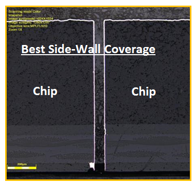 Figure 1: Excellent Throwing Power of Coating by Plating Technology.
Figure 2 shows the process flow of plating on mold compound which is proposed by Atotech’s standard process. Theoretically, shielding effectiveness of a material is contributed from three main loss mechanisms: reflection, absorption, and multi-reflection. When an incident wave travels to the shielding material, it is partially reflected with a portion of the wave penetrating into the material. The penetrated wave can propagate inside the material and get attenuated due to the absorption of the material. Once the remaining transmitted wave arrives at the other surface of the shielding material, the second reflection occurs and the wave gets bounced back, resulting in multiple reflections between the two surfaces of the shielding material.
| Surface preparation (cleaning and adhesion adhancement) |
↓
| Surface activation (conductive the surface) |
↓
| Electroless Ni/Cu (build the shielding layer) |
↓
| Electrolytic Ni or Cu or NiFe (higher speed plating for thickness requirement) |
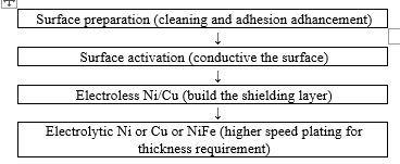 Figure 2: Process Flow of Plating on Mold Compound Shielding Effectiveness
Due to the fact that the wave is attenuated to 1/ e at one skin depth, the multi-reflection loss can be ignored for the cases where the shielding thickness is much larger than the skin depth. In summary, the shielding effectiveness in dB, SEdB is expressed in equation 1,
SE dB = R dB + A dB + M dB , (1)
where R dB is the reflection loss, A dB is the absorption loss, and M dB is the multi-reflection loss. Equation is further explained by Figure 3 [5].
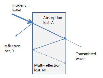 Figure 3: Electromagnetic Shielding Schematic Diagram
The reflection loss is
where Z0 represents the wave impedance of air and Z1 represents the wave impedance of the metal sheet. As
µ1and σ1 are the relative permeability and conductivity of the metal sheet, respectively, formula (2) can be estimated as
The reflection loss is directly proportional to the conductivity of the metal sheet but inversely proportional to the relative permeability of the metal sheet.
The absorption loss is
where L is the thickness of the metal sheet and
is the skin depth. Formula (5) can be estimated as
The absorption loss is directly proportional to the thickness, conductivity and relative permeability of the metal sheet.
The multi-reflection loss is
As Z>>Z1, formula (8) can be estimated as
If the thickness of the metal sheet is much larger than skin depth, incident wave will be attenuated significantly so that the multi-reflection loss will be negligible [6].
The EM shielding capability of a shield is escribed as shielding effectiveness, SE, which is defined as the ratio of the electric fields and magnetic field at a point without and with the shield as equation 10a and 10b,
where E1, H1 is the electrical and magnetic field at an arbitrary point without the shield, and E2, H2 is the electrical and magnetic field at the same point with the shield [7].
The shielding effectiveness value depends on the shielding material, its thickness, size of the shielded volume, grounding structures, and the frequency of interest.
2. Preparation of Test
In order to investigate the performance of metal plating on EMI sheilding, test matrixes are prepared with electrolytic plated nickel (pure nickel), electroless plated nickel (nickel-phophorous, P at 7-10%), and pure plated copper as the shielding layer on top of mold compound. For measurement of the electromagnectic field, a copper circuit is designed with substrate material Isola IS410, whereby the spiral flow is made on top of dielectric according to the specifications of ASTM D3123 (Figure 4).
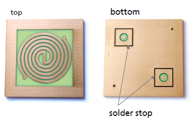 Figure 4: Spiral Circuit formed for near field EMI shielding test
Circuit is then encapsulated by mold compound Sumitomo EME_G770H Type F, with the leg connected to power input is located in opposite side of the dielectric. After that, the sample will go through the process as illustrated in Figure 5.
- Circuit pattering
- Encapsulate of mold compound
- Plating on mold compound
- Overall actual sample
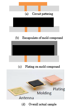 Figure 5: Preparation of test coupon.
From signal source, frequencies ranging from low to high frequency are loaded into the test coupon, magnetic field generated by spiral flow circuit is measured using the near field probe, and recorded in network analyzer. The setup of the experiment is shown in Figure 6.
| Network analyzer |
| Signal source |
| Near field probe |
- Setup of EMI shielding measurement
- Generated Field Distribution
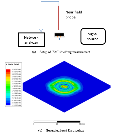 Figure 6: Shielding Effectiveness Measurement Setup
3. Experimental Results and Analysis
A series of samples with increasing thickness of plated Cu from lower to higher side, as indicated on Table 1 are fabricated and tested.
Table 1: Metal Thickness DOE
| Material | Thickness, um |
| Electroless Cu | 1 |
| Electrolytic Cu | 5, 10, 15 |
All data recorded by the plated samples with different thickness and materials is compared versus a control sample (sample without any plating on mold compound). The ratio of 2 readings is used for calculation of shielding effectiveness. Formula 10b is applied on these calculations.
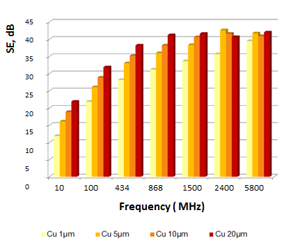 Figure 7: Shielding Effectiveness on Copper with various frequency test
On data analysis of metal shielding by copper (Figure 7), 4 samples are prepared, which are 1 um Cu sample plated by electroless Cu, 5um, 10um, 20um, samples are plated by electrolytic Cu. Higher electroless Cu thickness ( > 1um) s not prepared considering its high running cost and high leadtime during mass production. Signal input with frequency 10MHz, 100 MHz, 434 MHz, 868 MHz, 1.5 GHz, 2,4 GHz, and 5.8 GHz are tested. The experimental results show that shielding performance is improved by increasing the metal thickness, especially in lower frequency (< 1 GHz). At higher frequency, 5.8 GHz, thickness of Cu shows little impact on EMI shielding effectiveness. Hence further increasing is not helping to improve shielding effectiveness (SE) at high frequency range.
Similar test matrix is applied with nickel, shows in Table 2. Samples with electrolytic Ni 1 um, 3 um, and 5 um; as well as
electroless NiP 5um have been evaluated (5um NiP is reasonable in cost and can be plated within 25 min). Same signal input with frequency 10MHz, 100 MHz, 434 MHz, 868 MHz, 1.5 GHz, 2,4 GHz, and 5.8 GHz are applied to allowed the direct comparison. NiP is selected as matrix of study due to it is electroless process which required non conductive point. Besides, NiP with physical property of high hardness and good corrosion resistance make it suitable to be used as final surface.
Table 2: Metal Thickness DOE
| Material | Thickness, um |
| Electroless NiP | 5 |
| Electrolytic Ni | 1, 5, 10 |
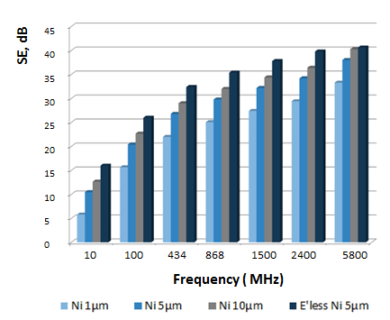 Figure 8: Shielding Effectiveness on Nickel with various frequency test
In gerenal, result from Figure 8 shows a more consistent trend for shielding effectiveness improvement over the thickness increase. Nickel alloy with phosporuos content is showing relatively better perfomance on SE versus pure nickel.
Comparing 1um and 5um of pure copper vs pure nickel at high frequency 5800 MHz, we see copper has higher SE (40dB) compare to nickel. As from equation 7, the absorption loss is directly proportional to the thickness, conductivity and relative permeability of the metal sheet. Electromagnetic radiation from the high frequency penetrates only at the near surface region of conductor layer. From equation 6, the skin depth, δ, decreases with increased frequency and increase conductivity and permeability. For copper, when relative conductivity, µr = 1, and σ = 5.8 x 10⁷ Ω-1m-1, δ = 2.43 x 10⁻⁹ at 5800 MHz; and for nickel, when relative conductivity, µr = 100, and σ = 1.15 x 10⁷ Ω-1m-1, δ = 0.547 x 10⁻⁹ at 5800 MH.
Table 3: Electrical conductivity relative to copper (σr) and relative magnectic permeability (µr) of selected material. [8]
Lower frequency shows a more challenging task to shield. In copper material, a maximum 40 dB can be obtain at frequency 5.8GHz at 5um thickness, but for 10mHz, the best shielding performance is only 22 dB at 20um thickness. By taking 5 um as benchmark to compare the material performance, Ni or NiP and Cu show close SE result at 5.8 GHz; but in lower frequency mode (10MHz) Cu and NiP are performing better than pure Ni; which Cu and NiP SE is 15 dB, versus pure Ni SE at 10 dB.
Our target to fulfill industrial requirement is to achieve minimum 30dB SE for varies high and low requency applications. Higher frequency interference is normally shielded by a thin conductive metallization layer. Simple electrically conductive layers however are transparent to low frequency magnetic fields, as shown in Figure 7. This low frequency magnetic interference can be emitted from sources such as switches, motors, power supplies, and transformers and is typically a challenging EMI shielding problem. If low frequency magnetic shielding is required ,it is normally achieved through the use of special ferromagnetic metal alloys with high magnetic permeability (see Figure 9). In order to further improve the SE on lower frequency signal device (such as radio), additional Ni/Fe alloy (Ni75/Fe25 in weigh percentage) is plated on top of Cu. Ni/Fe alloy with high ferromagnetic property can improve electromagentic shielding in low frequency mode.
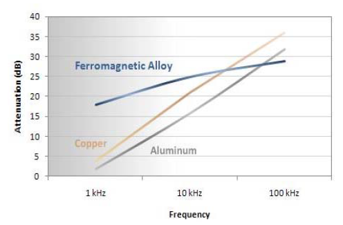 Figure 9 ‐ Magnetic shielding ability at different frequencies [8]
Materials with high magnetic permeability protect sensitive devices from the electrical noise caused by magnetic fields by redirecting the magnetic field through the shielding material and away from the protected device. In the same way, the devices that emits low frequency magnetic fields can also be isolated through the use of materials with high magnetic permeability. [9]
Table 4: Additional Metal Thickness DOE
| Matrix | Metal combination, um |
| 1 | 1um electroless Cu seed + 20um Electrolytic Cu + 4um Ni/Fe |
| 2 | 1um electroless Cu seed + 10um Electrolytic Cu + 4um Ni/Fe |
| 3 |
1um electroless Ni seed + 10um Electrolytic Cu + 4um Ni/Fe
|
| 4 |
1um electroless Ni seed + 20um Electrolytic Cu + 4um Ni/Fe
|
| 5 | 1um electroless Ni seed + 20um Ni/Fe |
New results showed that plated Cu in combination with ferromagnetic Ni/Fe gives significant improvement on shielding over low frequency signal (Figure 10). Combination of 1um electroless Cu seeding, plus 20um electrolytic Cu and with final finishing layer 4um of Ni/Fe could achieve 40dB of SE over the 10MHz wave. From the seeding method selection between electroless Cu and Electroless Ni, we notice electroless Cu gives slight better SE performance compare to electroless Ni, with around 3-4dB extra of SE. Plating 20of Cu give extra 6-7 dB SE compare to 10um Cu. Plating 20um Ni/Fe alone will give only 20dB of SE.
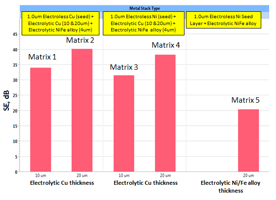 Figure 10: Shielding Effectiveness of Cu Plating combined with Ni/Fe alloy plating on Lower Frequency 10MHz
4. Conclusions
Plating on mold compound provides alternative option on EMI shielding with the proven reliability performance. The solution show features such as thin film coating capability, high throwing power in multiple dimension and high cost advantage compare to sputtering process. Selection of material and metal coating thickness are factors of EMI shielding effectiveness. Experiments show at high frequency of 5.8 GHz, shielding effectiveness as high of 35-40dB can be obtained by plating of elctrolytic Ni, electrolytic Cu or electroless NiP. Meanswhile, for lower frequency signal down to 10MHz, 35- 40dB SE can be achieved by electrolytic Cu plating and capped by 4um Ni/Fe alloy. With the correct combination on metals and thicknesses, conformal metal plating performs a good solution meeting EMI shielding’s requirement over high and low frequency.
Conflict of Interest
The authors declare no conflict of interest.
Acknowledgment
The authors would like to acknowledge the support of this work by Atotech USA, Atotech Berlin and Universiti Teknikal Malaysia Melaka (UTeM) in sharing the information, facilities and materials
- EMI Shielding Performance by Metal Plating On Mold Compound, 2016 IEEE 37th International Electronics Manufacturing Technology (IEMT) & 18th Electronics Materials and Packaging (EMAP) Conference
- ICSE 2014, [Adhesion Enhancement for Electroless Plating on Mold Compound for EMI Shielding with Industrial Test Compliance]
- Etnews, Korea IT news, Feb16, 2016, http://english.etnews.com/20160216200001
- Yi He, Jun Li, Gengxin Tian, Fengman Liu, and Liqiang Cao, IEEE Transactions On Electromagnetic Compatibility, Vol. 58, No. 2, April 2016 [Study on a Conformal Shielding Structure With Conductive Adhesive Coated on Molding Compound in 3-D Packages]
- Liao Kuo-Hsien, Alex, Chi-Hong, Chan, Shen Chia Hsien, Lin, I-Chia; Huang Hsin Wen, CPMT Symposium Japan, 2012 2nd IEEE [Novel EMI Shielding Methodology on Highly Integration SiP Module]
- Fankun Jiang, Ming Li, Liming Gao, 2014 IEEE, Research on conformal EMI shielding Cu/Ni layers on package, School of Materials Science and Engineering Shanghai Jiao Tong University.
- Nozad Karim, Jingkun Mao, Jun Fan 2010 Asia-Pacific International Symposium on Electromagnetic Compatibility, April 12 – 16, 2010, Beijing, China [Improving Electromagnetic Compatibility Performance of Packages and SiP Modules Using a Conformal Shielding Solution]
- DDL Chung, ASM International, 5 Jan2000 [Material for Electromagnetic Interference Shielding]
- Rich Emrich, September 21, 2010, Integran Technologies Inc., Toronto, ON [Low Frequency Magnetic Shielding – An Integrated Solution]