A High Efficiency 0.13μm CMOS Full Wave Active Rectifier with Comparators for Implanted Medical Devices
A High Efficiency 0.13μm CMOS Full Wave Active Rectifier with Comparators for Implanted Medical Devices
Volume 2, Issue 3, Page No 1019-1025, 2017
Author’s Name: João Ricardo de Castilho Louzadaa), Leonardo Breseghello Zoccal, Robson Luiz Moreno, Tales Cleber Pimenta
View Affiliations
Federal University of Itajubá, IEST, Itajubá – MG, Brazil
a)Author to whom correspondence should be addressed. E-mail: joaotande@yahoo.com.br
Adv. Sci. Technol. Eng. Syst. J. 2(3), 1019-1025 (2017); ![]() DOI: 10.25046/aj0203129
DOI: 10.25046/aj0203129
Keywords: Active Rectifier, CMOS Comparator, Medical Devices

Export Citations
This paper presents a full wave active rectifier for biomedical implanted devices using a new comparator in order to reduce the rectifier transistors reverse current. The rectifier was designed in 0.13μm CMOS process and it can deliver 1.2Vdc for a minimum signal of 1.3Vac. It achieves a power conversion efficiency of 92% at the 13.56MHz Scientific and Medical (ISM) band.
Received: 30 April 2017, Accepted: 29 June 2017, Published Online: 11 July 2017
1 Introduction
This paper is an extension of work originally presented in The 15th International Symposium on Integrated Circuits, Sigapure, 2016 [1]. It presents some details not described in the original paper. This paper also brings new results obtained after a new calibration of the system that improved the circuit efficiency. Implanted medical device is a technology that offers several possibilities to improve medicine and it can change the paradigm of how doctors and patients deal with treatments and drugs. In order to be implanted, a medical devices need a source of power that will provide energy to the circuit. As used in RFID technology, one of the ways to supply power to implanted medical device is by using an inductive link [2] that can power up a circuit through the skin without to use transcutaneous wires, which could expose the patient to bacterias and viruses [3]. The other solution is by using batteries that have limited life and can cause heavy metal contamination in case of leakage.
An inductive link requires an AC-DC rectifier that is responsible to transform the signal wave into a power supply. Rectifiers are usually designed to use conventional diodes that have a built drop voltage of
Although this work is focused on inductive links, there are other ways to transfer energy. There are some applications that use ultrasound waves to excite a piezoelectric device to generate a current. Another way to provide power to medical implants is by using a thermoelectric generator that makes use of the temperature gradient between inside and outside of body to create energy by Seebeck Effect.
0.7V, which is suitable for conventional applications but it is unusable for circuits running on power supplies of 1V or less. Alternatively to the conventional diodes, Schottky diodes can be used, but the manufacturing process of low forward drop voltage can be more expensive than the traditional processes [4] because they might not be present in some regular processes and require extra fabrication steps [5]. An alternative is the use of diode connected MOS transistors to replace the conventional diodes in a bridge connection. CMOS transistors connected as diodes can work at high frequencies, such as the Scientific and Medical – ISM band (13.56MHZ) that has been widely used [4, 5, 6]. One problem of this solutions is that diode connected MOS transistors in a bridge connection offers low ON-OFF switching speed which in turn creates an undesirable reverse current. A cross-coupled connected structure (Figure 1) can make the operation more efficient and minimizes the reverse current, but in the ideal case the ON-OFF switch of the CMOS transistors would be controlled by another circuit that can speed up the operation and can create a dynamic rectifier to make the operation more efficient, thus minimizing the reverse current. Some dynamic rectifiers have been reported in the last few years [6, 7, 8] as solutions for powering medical devices under low power.
One important characteristic of power supply is the power conversion efficiency (PCE), equation 1, which is defined as the rate of the energy dissipated by the load by the power consumed by the entire circuit
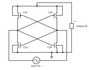 Figure 1: Cross-Coupled Rectifier [9]
where ηpa, ηlink, ηrectif ier, ηregulator represents the power amplifier, inductive link, rectifier, and regulator efficiency respectively. The ηrectif ier represents the amount of power provided to the output divided by the amount of power that enters in the rectifier (equation 2). For a PCE of 30% it is expected to have around 80% of efficiency of the AC-DC converter [6].
P CE = ηpa ∗ ηlink ∗ ηrectif ier ∗ ηregulator (1)
P out DC
ηrectif ier = (2)
P out AC
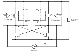 Figure 2: Active Rectifier Circuit [6].
The rectifier of Figure 2 is comprised of PMOS transistors Q1 and Q2, and NMOS transistors Q3 and Q4. Transistors Q5, Q6, Q7, and Q8 work in order to tie the PMOS base transistor always at the higher voltage [11]. Transistors Q3 and Q4 are connected as a cross-coupled gate structure while Q1 and Q2 are driven by comparators C1 and C2.
This paper presents one active rectifier using diode connected CMOS transistors, in 0.13µm process, controlled by two original comparators that are responsible for turning ON-OFF the circuit and minimize the reverse current. This work was intended to provide an output voltage of at least 1V.
2 Cross Couple Structure
The cross-coupled structure shown in Figure 1 connects the transistors gates in a cross mode. That configuration puts the gates of transistors CQ1 and CQ2 biased at a positive signal when their drain are biased by the negative signal. On the other hand, when the circle change, the drains are biased by the positive signal and the gates by the negative signal. The transistors are made to turn ON at different voltage levels in their gates. NMOS needs to have high voltage and PMOS needs to have low voltage. At the same time the cross coupled circuit is designed so that the PMOS transistors provide higher voltage to the load while NMOS provide the lower voltage or GND voltage.
3 Active Rectifier
As mentioned in the introduction section, the desirable rectifier should have a minimal reverse current, and one widely used way to achieve it is by using a comparator that can turn the rectifier ON-OFF faster enough. The Figure 2 shows the schematic of the rectifier [6].
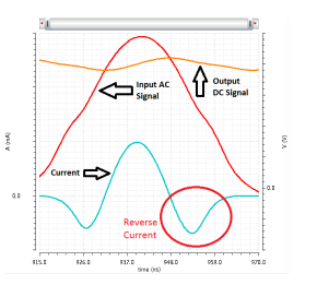 Figure 3: Cross-Coupled Rectifier wave form.
While the cross-coupled rectifier has a considerable reverse current (Figure 3) the two comparators shown in Figure 2 allow the active rectifier to switch faster and minimize it. The challenge faced by this technology is to make the comparators work fast enough. Figure 4 shows the waveform signals and highlights the comparator signal delay by circles C and B, as well as the reverse current, by circle A.
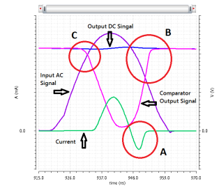 Figure 4: Active Rectifier waveform – (A) reverse current, (B) output delay, (C) entry delay.
In the ideal case, a perfect comparator would start its output signal a moment before the AC signal became larger than DC signal and would finish the pulse in the exactly moment the AC signal becames smaller than the DC signal. It is possible to see in the Figure 4 the delay showed inside of circle B which creates the reverse current in circle A.
4 Two Input Common Gate
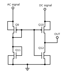 Figure 5: Two input common gate.
Figure 5 shows the Two Input Common Gate Comparator, which is the comparator used to develop the proposed comparator. This comparator is used in order to monitor AC and DC signals, and to switch ON and OFF the rectifier transistors always when the AC signal becomes larger or smaller than the DC signal. The Two Input Common Gate uses only four transistors, Q10 and Q12 that form an inverter, and Q9 and Q11 that form a voltage divider responsible by create an (AC signal)/2. That comparator has been used since it is small and simple, it does not require external power source, it consumes low power and provides faster switch for the rectifier transistors than a cross couple structure. Although that comparator is relatively fast, we propose a new comparator based on the Two Input Common Gate, with some modifications that speeds up the operation of the switching transistors.
5 Proposed Comparator
The proposed comparator shown in Figure 6 is a modified version of the two-input common gate, with an extra capacitor and an extra voltage divider that are responsible for speeding up the comparator.
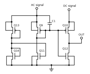 Figure 6: Proposed Comparator.
Transistors Q9, Q10, Q11, and Q12 form a modified common gate structure. The gate of transistor Q11 is connected to Q13 and Q14. Transistors Q10 and Q12 compose an inverter that can bring the OUT pin to low or high level (DC signal). The transition between high and low level happens when the voltage, at Q10 and Q12 gates, is larger than half of DC signal. Our comparator aims to detect when AC signal is larger than DC signal. In order to accomplish it, transistors Q9 and Q11 form a voltage divider designed to put the gates of Q10 and Q12 at a voltage larger than DC/2 in the moment that AC signal is larger than the DC signal.
In the proposed comparator, capacitor C1 works in order to improve the rise time of the signal provided by the voltage divider formed by Q9-Q11. While C1 is not charged, it works as a short circuit and allows the AC signal to drive the Q10-Q12 inverter. When C1 is charged, it becomes an open circuit, and the voltage between Q9 and Q11 starts to drive the inverter. Figure 7 Q10-Q12 gates voltage waveform inside of the circle. A lump appears when C1 gets full and disconnects the AC signal from driving the inverter. The lump can occur above or below in the signal according to the value of capacitor C1. If C1 is larger than a certain value it will stop decreasing the reverse current and will start increasing it. Figure 8 (a) shows a waveform with an acceptable capacitor and (b) with a capacitor larger than the optimum point. Figure 8
(b) does not have a lump since its capacitor C1 is so big that it never gets fully charged, and the AC signal drives the inverter the whole time.
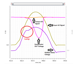 Figure 7: Proposed Comparator waveform. Lump’s highlight.
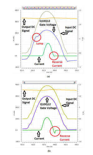 Figure 8: Comparative between waveforms using an acceptable capacitor size (a) and an over sized capacitor (b).
Capacitor C1 helps the circuit to work faster but the use of integrated capacitor can be a problem since it may take a lot of silicon area. In order to avoid it, a second voltage divider is used. The voltage between transistors Q13 and Q14 is designed to be just a little higher than the voltage between transistors Q9 and Q11. It allows transistor Q11 to turn ON a little earlier and to provide the delay shown in Figure 4 circle B to be a little shorter. Just as a comparison, if capacitor C1 is 10pF at 1.3Vac input signal voltage, the maximum reverse current, without the voltage divider, is almost 2 times larger than the use of a voltage divider. In order to have the same result without to use the voltage divider, capacitor C1 would need to be 97pF.
6 Details About the Capacitor
In order to choose an ideal size of capacitor, some considerations taken into account. The capacitor size depends on the resistance and on the frequency operation, which defines the time the capacitor needs to get fully charged. Since the circuit resistance changes during the circuit operation, the maximum capacitance will be calculated, and later a smaller capacitance value needs to be calibrated through simulations. The τ constant shown in equation 3 relates capacitor load time to the circuit resistance and capacitance
τ = RC (3)
During the time given by the RC constant, a capacitor gets 63% charged/discharged [12]. For a 99.3% load, it takes 5τ [13]. If a charge time of T = 5τ replace τ at equation 3 then the equation 4 will provide capacitance that can be used in the circuit.
T
C = (4)
5R
In order to obtain the time T on equation 4, the circuit frequency needs to be analyzed. The time for the capacitor be fully charged needs to be less than the time to signal AC changes from zero to the maximum voltage value. That time is exactly 1/4 of the cycle time. For 13.56MHz, it is 0.0184µs.
In order to determine the resistance R, the Thevenin method for equivalent resistance can be used. The R resistance applied to equation 4 results in a reference capacitance that needs to be calibrated by simulations. Its occurs because the R resistance is not constant in this circuit.
7 Type of Transistor
In this work halo implanted transistors of small channel were used. Although this kind of transistor has some problems such as threshold voltage mismatch, caused by the halo implant, [14] they offer the advantage of having less internal resistance [14]. This smaller internal resistance helps the circuit to waste less energy on its own operation.
8 Transistors Sizing
The transistors sizing takes 4 steps. The first step is used to obtain the current to be provided by the rectifier transistors. This amount of current sets the minimum size of the four rectifier transistors according to the technology used. After selecting the size of the four rectifier transistors, the others three steps are related with the comparator.
In the second step 2, transistors Q10 and Q12, which form the inverter are chosen. Those transistors need to be large enough to supply current to the rectifier. Besides that, Q10 and Q12 need to be designed to switch the inverter exactly at half of the DC signal voltage.
The next step would be the design of transistors Q9 and Q11 that form the main voltage divider and provide voltage to the inverter. Nevertheless, since the gate of Q11 is controlled by Q13 and Q14, the auxiliary voltage divider, therefore the voltage divider Q13Q14 needs to be designed first.
While the main voltage divider needs to provide a voltage of (AC signal)/2 to the inverter, the auxiliary voltage divider needs to provide a voltage larger than (AC signal)/2 to the gate of Q11 in order to turn it on a little earlier. Thus, in step 3 the voltage divider Q13Q14 needs to be designed to provide voltage ((AC signal)/2 + δ). In our work we have chosen δ = 100mV, but a different voltage is acceptable.
The fourth step, after designing the inverted and the auxiliary voltage divisor, the main divisor needs to be designed to provide (AC signal)/2 voltage. Since the auxiliary voltage divider controls the gate of Q11 it can be a little difficult to obtain the Q9 and Q11 sizes. A simulation tool can help this task.
After the 4 steps, the capacitor needs to be calculated, as described in section 6.
Figure 9 summarizes all the steps described in this section.
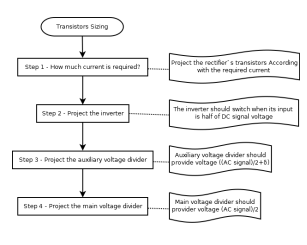 Figure 9: Transistors Sizing Flowchart.
9 Results
In order to simulate an input sine-wave at 13.56MHz, of 1.3V peak was used.
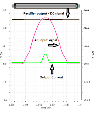 Figure 10: Output of wave form using the proposed comparator.
Figure 10 shows the output waveform. The output DC voltage is 1.2V and the output peak current is 55.55mA under a reverse current of -1.47mA. In order to trace this curve, a capacitor of 20nF and a resistor of 193 ohms were connected in parallel as load [6].
PCE.
Table 1: Comparison with previous works. |
The maximum ηrectif ier obtained is 0.92 and it was computed using the same method described in [6] that can be obtained from equation 2. The curve of input voltage vs PCE is shown in Figure 11.
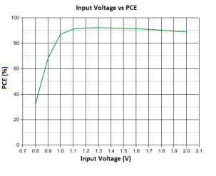 Figure 11: Relationship between input and output voltage.
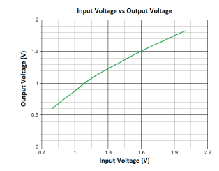 Figure 12 shows the relationship between input and output voltage.
Table 1 shows a comparison to other works. It is possible to verify the PCE achieved was compatible with other reported rectifiers and that the output voltage is compatible with implantable devices.
10 Conclusion
In this extended version it is presented a low power rectifier, on a new operating condition, using a proposed comparator. The comparator is intended to reduce the switching delay of the rectifier transistors, in order to decrease the reverse current. It was accomplished by using an extra capacitor and an extra voltage divider as compared to the original twoinput common gate comparator. Those comparator and rectifier were designed and simulated on 0.13µm CMOS process. The circuit was designed to work at 13.56MHz with an input signal of at least 1.3Vac. The rectifier efficiency increased by 10% when compared to the original paper and it can achieve a 92% of maximum efficiency at 1.2V.
Conflict of Interest
The authors declare no conflict of interest.
Acknowledgment
This work was supported by FAPEMIG, CNPq and CAPES.
- J. R. C. Louzada, L. B. Zoccal, R. L. Moreno, and T. C. Pimenta, “A 0.13μm CMOS full wave active rectifier with comparators for implanted medical devices,” in 2016 International Symposium on Integrated Circuits (ISIC), Dec 2016, pp. 1–4.
- M. Ghovanloo and K. Najafi, “A wideband frequency-shift keying wireless link for inductively powered biomedical implants,” IEEE Transactions on Circuits and Systems I: Regular Papers, vol. 51, no. 12, pp. 2374–2383, Dec 2004.
- P. T. Theilmann, “Wireless power transfer for scaled electronic biomedical implants,” Thesis, University of California San Diego, 2012.
- Y. H. Lam, W. H. Ki, and C. Y. Tsui, “Integrated low-loss CMOS active rectifier for wirelessly powered devices,” IEEE Transactions on Circuits and Systems II: Express Briefs, vol. 53, no. 12, pp. 1378–1382, Dec 2006.
- H. M. Lee and M. Ghovanloo, “An integrated power-efficient active rectifier with offset-controlled high speed comparators for inductively powered applications,” IEEE Transactions on Circuits and Systems I: Regular Papers, vol. 58, no. 8, pp. 1749– 1760, Aug 2011.
- H.-K. Cha and M. Je, “A single-input dual-output 13.56 MHz CMOS AC–DC converter with comparator-driven rectifiers for implantable devices,” Microelectronics Journal, vol. 45, no. 3, pp. 277 – 281, 2014. [Online]. Available: http://www. sciencedirect.com/science/article/pii/S0026269214000135
- Y. Lu and W.-H. Ki, “A 13.56 MHz CMOS active rectifier with switched-offset and compensated biasing for biomedical wireless power transfer systems,” IEEE Transactions on Biomedical Circuits and Systems, vol. 8, no. 3, pp. 334–344, June 2014.
- R. Ramzan and F. Zafar, “High-effciency fully cmos vco rectifier for microwatt resonant wireless power transfer,” IEEE Transactions on Circuits and Systems II: Express Briefs, vol. 62, no. 2, pp. 134–138, Feb 2015.
- L. Yao, J. H. Cheong, R.-F. Xue, and M. Je, “An inductive coupling based CMOS wireless powering link for implantable biomedical application,” world academy of science, engineering and technology, vol. 69, pp. 456–459, 2012.
- A. Khalifa, “Study of CMOS rectifers for wireless energy scavenging,” Thesis, Linköping University, Electronic Devices, The Institute of Technology, 2010.
- H. K. Cha, W. T. Park, and M. Je, “A CMOS rectifier with a cross-coupled latched comparator for wireless power transfer in biomedical applications,” IEEE Transactions on Circuits and Systems II: Express Briefs, vol. 59, no. 7, pp. 409–413, July 2012.
- Federal University of Uberlândia, “Charging and Discharge of a Capacitor,” http://www.facip.ufu.br/sites/facip.ufu.br/files/Anexos/Bookpage/fe3-06-carga-e-descarga-de-um-capacitor.pdf, acessado: 13 jan. 2017.
- M. A. Cavalcante, C. R. C. Tavolaro, and E. Molisani, “Physics with Arduino for beginners,” Revista Brasileira de Ensino de Física, vol. 33, pp. 4503 – 4503, 12 2011.
- G. D. C. Colletta, “An asynchronous sigma-delta modulation architecture in ultra-low power for biomedical applications.” Theses, Federal University of Itajubá, 2015.