Structural Optimization of Wavy FinFET for Leakage Reduction and Performance Enhancement
Structural Optimization of Wavy FinFET for Leakage Reduction and Performance Enhancement
Volume 2, Issue 3, Page No 913-917, 2017
Author’s Name: Anju Chakkikavil1, a), Nisha Kuruvilla1, Ayoob Khan1, Shahul Hameed2
View Affiliations
1Department of Electronics Engineering, College of Engineering Chengannur, 689121, India
2Department of Electronics and Communication Engineering, TKM College of Engineering, 691005, India
a)Author to whom correspondence should be addressed. E-mail: anjucraman@gmail.com
Adv. Sci. Technol. Eng. Syst. J. 2(3), 913-917 (2017); ![]() DOI: 10.25046/aj0203114
DOI: 10.25046/aj0203114
Keywords: FinFET, Ultrathin Body, Wavy, SOI, Leakage, Spacer

Export Citations
Wavy FinFET is a hybrid device that integrates FinFET and Ultrathin Body FET technologies on SOI platform to provide high density and drivability without causing area penalty. The problem associated with this device is higher leakage and lower threshold voltage. This problem can be solved by structural modification of the device. This work analyses the performance of Wavy FinFET under various optimization methods such as device/channel engineering, work function engineering, spacer engineering and variation of isolation oxide thickness. The obtained results indicate that optimized Wavy FinFET can act as a solution for low power, highly reliable device topology. Leakage power is found to be reduced by 40.39%, 30.39% and 43.75% with channel engineering techniques such as substrate doping., halo doping and retrograde doping, respectively. Leakage power is lowered by 35.48% and 32.25% with increase in gate work function and isolation oxide thickness respectively. By using high k spacer material 54.77% reduction in leakage is further obtained without compromising drive current. In ADSE(Asymmetric Drain Side Extention) wavy FinFET,leakage is reduced by 61.35%. Whereas in symmetric and asymmetric Dual k wavy FinFET, leakage reduction is found to be 44.19% and 28.25% respectively.
Received: 05 April 2017, Accepted: 24 May 2017, Published Online: 30 June 2017
1. Introduction
Gordon Moore predicted the scaling trends in integrated circuits in 1965 [1]. The technology driving factors are reduced cost, improved performance and greater circuit functionality. Scaling causes reduction in gate control over current flow in channel and which will in turn results in short channel effects. In order to mitigate these effects, engineers had to innovate advanced MOSFET structures which can be used in smaller technology nodes. Gate oxide scaling combined with gate length scaling was the traditional MOSFET scaling which ran out in the early 2000’s due to leakage limitations. Engineers had to innovate new structures since market was demanding low leakage. Strained silicon is an example of a revolutionary technology that provided improved performance when traditional MOSFET scaling methods were no longer effective [2]. It provided valuable performance enhancements at 90 nm and 65 nm generations. Intel’s 45 nm logic technology was the first to introduce high-k + metal gate transistors for improved performance and reduced leakage [3]. Further scaling was achieved using structural change in transistor architecture. A layered silicon-insulator-silicon substrate replaced conventional silicon substrates to form SOI technology[4]. The ultrathin body FET eliminates the leakage paths between source and drain , and thereby control short-channel effects with thin body [5]. Multiple gate devices such as double gate, trigate, pi-gate, GAA devices could achieve better gate control over channel [6]. ITFET (Inverted T channel FET) combines double gate FinFET and single gate SOI to achieve layout efficiency[7].
Wavy FinFET is a hybrid device comprising of FinFET and Ultrathin body FETs [8]. Since UTB (Ultrathin Body) is inserted in the otherwise wasted fin-fin spacing, drivability increases (because of the increased path for current flow ) without causing area penalty. The major issues related to wavy FinFET architecture are increase in leakage and reduction in threshold voltage. Optimization are required to mitigate these problems and thereby to obtain better device performance.
In the following session, comparative analysis of trigate SOI FinFET and wavy FinFET are done. After that optimization methods such as channel engineering, work function engineering, spacer engineering and isolation oxide thickness variation are done. Finally the last session concludes this work.
2. Trigate v/s Wavy FinFET
3D structure of Trigate SOI FinFET, segmented trigate SOI FinFET with 3 fins and wavy FinFET having dimensions as per 2013 Overall Roadmap Technology Characteristics Fin-FET parameters specified by the International Technology Roadmap for Semiconductors (ITRS) at the 7-nm technology node [9] were drawn using COGENDA TCAD [10]. In all structures fin height width and fin termination edge are 30nm, 6.8nm and 25nm respectively. Gate length is 18nm and EOT is 0.5nm. The channel is intrinsic and UTB thickness in wavy FinFET is 4.5nm. Fin spacing is 19nm in the case of multifin architecture. The structures are given in Figure 1. It can be seen that Ultrathin body is inserted in the otherwise wasted fin spacing to achieve advantages of two competing technologies. Figure 2 shows the gate cross section of trigate FinFET with single fin, with 3 fins and that of wavy FinFET. We can see that channel area under gate in wavy FinFET is higher compared to that of conventional FinFET.
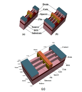 Figure 1.(a) Trigate FinFET with single fin, (b) Trigate FinFET with 3 fins, (c) Wavy FinFET
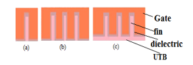 Figure 2. Gate cross section of (a) Trigate FinFET with single fin, (b) Trigate FinFET with 3 fins and (c) Wavy FinFET
Simulations are carried out to analyase the performance of normal trigate FinFET with single fin, trigate FinFET with multiple fins and wavy FinFET. Also the Ultrathin body thickness is varied from 2.5nm to 4.5nm to see the variation of current with ultrathin body thickness. In Table 1, W2.5, W3.5, W4.5 represents wavy FinFET with UTB thickness 2.5nm, 3.5nm, 4.5nm respectively.
Table 1. Comparison of conventional FinFET and wavy FinFET (UTB thickness=2.5nm, 3.5nm, 4.5nm)
|
Stru Cture |
Ioff (A) |
Ion (A) |
Vt (mV) |
SS (mV/dec) |
DIBL |
|
trigate 1 fin |
2.05e-13 | 1.03e-05 | 372 | 62 | 40 |
|
trigate 3 fins |
3.21e-13 | 2.43e-05 | 371 | 62.8 | 40.2 |
| W 2.5 | 1.09e-12 | 2.79e-05 | 367 | 65.7 | 43.6 |
| W 3.5 | 3.35e-12 | 2.95e-05 | 365 | 70.2 | 47.3 |
| W 4.5 | 1.55e-11 | 3.82e-05 | 355 | 73.9 | 53 |
It can be seen that the drive performance of segmented FinFET is better than that of conventional FinFET. In order to increase the drive current further, it is required to array more number of fins which will result in area penalty. At the same time wavy FinFET overcomes this difficulty and current is increased keeping the same footprint area. Also it is found that drive capability and short channel characteristics varies with the thickness of UTB in wavy FinFET. It can be seen that, higher UTB thickness results in ION. But the problem is along with ON current, OFF current also increases. Threshold voltage of wavy FinFET is lesser compared to that of conventional FinFET which further reduces with increase in UTB thickness.
Due to threshold voltage mismatch between UTB and fins, subthreshold swing and DIBL becomes higher in wavy channel transistor. Hence wavy FinFET has to be optimized to achieve higher ION with lower leakage power.
- Optimized Low Power Wavy FinFET
Substrate back biasing is one of the methods for threshold voltage tuning [8]. Reverse back biasing helps to increase the Vt and reduce IOFF. The problem here is that the reduction in leakage is obtained at the expense of ON current. Hence another methods are needed to optimize wavy FinFET, which is discussed in the following sessions of this work.
3.1. Substrate Doping
Doping concentration of the silicon is varied from undoped to 1e17 cm-3. Fig. 3 represents the variation in Vt with doping concentration. Vt increases as doping increases. Table 2 represents the effect of doping on ION, IOFF and leakage power. Both linear and logarithmic plot of Vgs– Id characteristics with different doping concentration are shown in Figure 4. It can be observed that along with increase in doping concentration, leakage is reduced. Hence leakage power is also reduced. 40.39% reduction in leakage current is obtained by choosing the doping concentration to be 1e17/cm3. Here a 4.71% reduction in ON current is observed.
Table 2. Effect of doping
|
Doping (cm-3) |
Ioff (A) |
Ion (A) |
Pleak (W) |
| Undoped | 1.55e-11 | 3.82e-05 | 1.24e-11 |
| 1e16 | 9.79e-12 | 3.67e-05 | 7.83e-12 |
| 1e17 | 9.24e-12 | 3.64e-05 | 7.39e-12 |
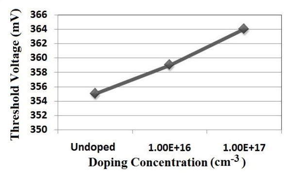 Figure 3. Vt variation with doping concentration
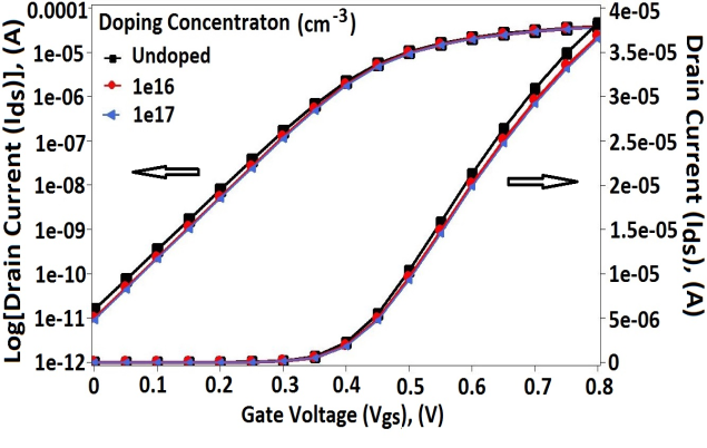 Figure 4. Transfer characteristics with different doping concentration
3.2. Halo and Retrograde Doping
Halo doping can be performed by incorporating highly doped p type region near source and drain ends. Here the drain and source junction depletion region width reduces. It can help in the reduction of DIBL (Drain Induced Barrier Lowering) and punch through. For retrograde doping surface concentration is kept low to increase surface mobility and the subsurface doping is kept high to act as a barrier against punch through [11]. Effect of both halo doping and retrograde doping are shown in Figure 5 and Table 3. By using these methods leakage can be reduced.
Table 3. effect of halo and retrograde doping
| undoped | Halo doping |
Retrograde Doping |
|
| Ioff | 1.55e-11 | 1.079e-11 | 8.718e-12 |
| Ion | 3.82e-05 | 3.72e-05 | 3.696e-05 |
| Pleak | 1.24e-11 | 8.632e-12 | 6.968e-12 |
| DIBL | 53 | 48 | 45.8 |
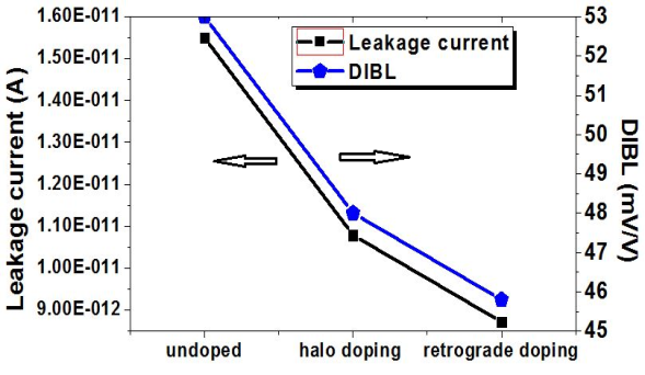 Figure 5. Effect of Halo and retrograde doping
Here the advantage is that we get reduction in leakage power without much sacrificing drive performance. Ion/Ioff ratio also will be higher.
3.3. Work function Engineering
Threshold voltage is dependent work function. Hence by varying gate work function of wavy FinFET, better performance can be achieved. Gate work function is varied from 4.5eV to 4.6 eV. Effect of work function is shown in Figure 6 and Table 4. As the work function increases, threshold voltage increases and leakage reduces. 35.48% reduction in leakage power is obtained by increasing work function to 4.6 eV.
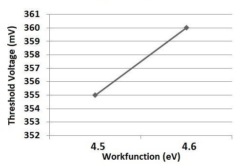 Figure 6. Effect of work function on Vt
Table 4. Effect of work function on performance of wavy FinFET
| Work Function(eV) |
Ioff (A)
|
Ion(A) |
Vt (mV) |
Pleak(W) |
| 4.5 | 1.55e-11 | 3.82e-05 | 355 | 1.24e-11 |
| 4.6 | 1.00e-11 | 3.73e-05 | 360 | 8.00e-12 |
3.4. Isolation oxide thickness variation
This is a method for leakage suppression. Threshold voltage is directly proportional to isolation oxide thickness. Increasing isolation oxide thickness leads to higher threshold voltage which further leads to reduced leakage. Isolation oxide thickness is varied from 20nm to 40nm. Effect of BOX thickness variation is given in Figure 7. Leakage power is found to be lower in the case of higher oxide thickness.
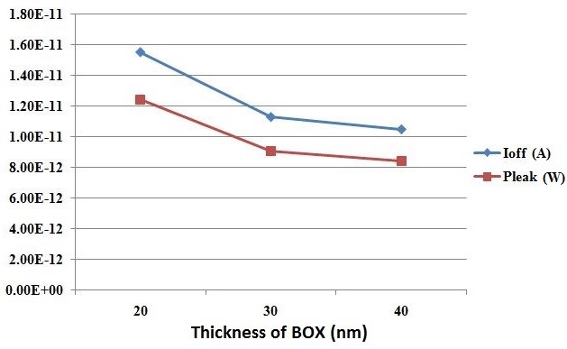 Figure 7. Effect of isolation oxide thickness on Ioff and leakage power
3.5. High-k Spacer
In sub-20 nm region, short channel effects are reduced using underlap regions. But here on current reduces. Even at high Vds, gate-source/drain barrier restricts source to drain carrier flow. Introduction of high-k spacers can provide strong field coupling from the gate. Effect change in spacer material is checked by using SiO2 (k=3.9), Si3N4 (k=7.5) and Hfo2 (k=22) as the spacers. Simulation result is shown in Figure 8. As the dielectric constant of the spacer material increases, an increase in Ion and reduction in Ioff can be seen. And thus device can be optimized for lower leakage power and higher Ion/Ioff ratio. Effect of change in spacer material on Ioff, Ion, Vt and leakage power is shown in Table 5.
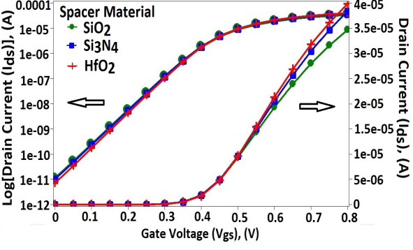 Figure 8. Transfer characteristics of wavy FinFET with different spacer materials
Table 5. Effect of change in spacer material
| Material | Ioff(A) | Ion(A) | Vt(mV) | Pleak |
| SiO2 | 1.09e-11 | 3.46e-05 | 356 | 8.72e-12 |
| Si3N4 | 1.01e-11 | 3.84e-05 | 362 | 8.08e-12 |
| HfO2 | 7.01e-12 | 3.98e-05 | 396 | 5.61e-12 |
Higher the dielectric strength of spacer, lesser the leakage, and higher the threshold voltage can be obtained which leads to a better device performance. By using HfO2 as the spacer material on both sides of gate, 54.77% reduction in off current is achieved.
3.6. Asymmetric Drain Spacer Extention (ADSE) Wavy FinFET
In asymmetric drain spacer extention FinFET as shown in Figure 9, an additional spacer is introduced only on the drain side to introduce drain-side underlap in FinFET. Thus, bidirectional currents in these transistors are not the same. The spacer thickness at drain side is higher which will result in asymmetry in current and reduction in DIBL. DIBL and OFF current is found to be reduced by using ADSE structure.
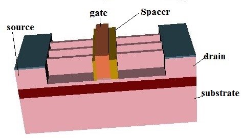 Figure 9: ADSE Wavy FinFET
Effect of ADSE wavy FinFET on drain current is shown in Figure 10. Drain current in logarithmic scale is shown on left Y axis and from which it can be understood that the OFF current is lower in ADSE Wavy FinFET compared to normal wavy FinFET. Here the leakage power is reduced by 61.35% compared to that of normal wavy FinFET.
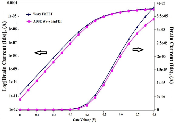 Figure 10: Effect of ADSE Wavy FinFET
3.7. Symmetric and Asymmetric Dual-k Spacer Architecture
The problem associated with high-k spacer is that it increases the fringe capacitance (Cfr) that worsens the circuit delay in digital applications [12]. By introducing dual k spacer, instead of single spacer material, inner high-k and outer low-k spacer material is introduced. Interface region between high-k and low k region can make significant changes in device properties. Ion/Ioff can be increased.
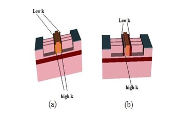 Figure 11: (a)Symmetric dual-k and(b)asymmetrc dual-k wavy FinFET.
In symmetric dual-k as shown in Figure 11(a), there will be dual k spacer on both sides of gate. Where as in asymmetric dual k structure as shown in Figure 11(b), dual k spacer is present only on source side. Effect of introducing symmetric dual-k spacer on leakage power and Ion/Ioff ratio are shown in Figure 12. For dual-k, Si3N4 and HfO2 are used as high k spacers along with SiO2 spacer. 44.948% increase in ION/IOFF is obtained with symmetric dual-k structure (HfO2- inner high-k spacer) compared to conventional with SiO2 spacer.
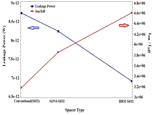 Figure 12: Effect of symmetric dual-k structure
Table 6 shows the effect of introducing asymmetric dual k spacer in wavy FinFET architecture. 28.25% reduction in leakage power is achieved by introducing asymmetric double dielectric spacer in wavy FinFET architecture
Table 6: Effect of asymmetric dual k spacer
| Structure | IOFF(A) | ION(A) | ION/IOFF |
Pleakage
|
| Wavy FinFET | 1.55e-11 | 3.82e-05 | 2.46e06 | 1.24e-11 |
|
Asymmetric dual k |
1.11e-11 | 3.76e-05 | 3.38e06 | 8.89e-12 |
3. Conclusion
Since wavy FinFET is a hybrid structure of UTBFET(Ultrathin Body FET) and FinFET, it is found to be better than conventional FinFET in terms of drivability, integration density and area efficiency. The problems associated with wavy FinFET are increased leakage power and degraded SCE. This work could propose structural modifications of wavy FinFET using methods such as channel engineering, work function engineering, variation of isolation oxide thickness and spacer engineering to optimize the device for better performance. ION/IOFF ratios of optimized structures are given in Figure 13 and Percentage change in leakage power is shown in Table 7. It can be observed that these optimization techniques leads to reduction in leakage and improvement in performance of wavy FinFET.
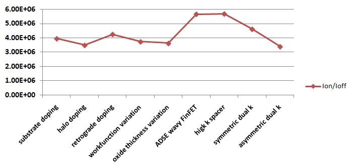 Figure 13: ION/IOFF in various optimization methods.
Table 7: Percentage change in leakage power and on current with optimization methods
| Methods | Value/Percentage reduction in Pleakage |
| Unoptimized Wavy FinFET | 1.24e-11 |
| Substrate Doping | 40.39% |
| Halo Doping | 30.39% |
| Retrograde Doping | 43.75% |
| Work function Engineering | 35.48% |
| BOX thickness Variation | 32..25% |
| Higk k spacer | 54.77% |
| ADSE wavy FinFET | 61.35% |
| Symmetric dual-k spacer | 44.19% |
| Asymmetric dual-k spacer | 28.25% |
Acknowledgment
This work was carried out by utilizing resources acquired by College of Engineering, Chengannur, through funded project granted by Department of Science Technology –India (DST-FIST Type-0).
- Gordon E. Moore, “Cramming more components onto integrated circuits”, https://doi.org/10.1109/N-SSC.2006.4785860
- Tatjana Pesic-Brdanin, Branko L. Dokic, “Strained Silicon Layer in CMOS Technology”, Electronics, vol. 18, no. 2, , 63-69, 2014. doi:10.7251/ELS1418063P
- M. Bohr, “The evolution of scaling from the homogeneous era to the heterogeneous era,” in Proc. IEEE Int. Electron Devices Meeting, 2011, pp. 1.1.1–1.1.6. https://doi.org/10.1109/IEDM.2011.6131469
- Yuan Taur , “Fundamentals of Modern VLSI Devices”
- Y.-K. Choi et al., “Ultrathin-body SOI MOSFET for deep-sub-tenth micron era,”IEEE Electron Device Lett., vol. 21, no. 5, 2000, pages. 254–255. https://doi.org/10.1109/55.841313
- Jong-Tae Park et.al, “Multiple-Gate SOI MOSFETs:Device Design Guidelines”, IEEE transactions on electron devices, vol. 49, no. 12, 2222-2229, 2002,. https://doi.org/10.1109/TED.2002.805634
- W. Zhang et.al, “The ITFET: A novel FinFET-based hybrid device,”IEEE Trans. Electron Devices, vol. 53, no. 9, 2006, pages. 2335–2343.
- Hossain M. Fahad et.al, “Simulation Study of a 3-D Device Integrating FinFET and UTBFET”, in press. https://doi.org/10.1109/TED.2014.2372695
- Overall Roadmap Technology Characteristics, ITRS,2013 [Online]. Available:http://www.itrs.net/links/2013ITRS/2013Tables/2013ORTC_Detailed Table.pdf, accessed Nov. 25, 2014
- VisualTCAD Semiconductor Device Simulator Version 1.7.2 VisualTCAD User’s Guide:Available :http://www.cogenda.com
- Kausik Roy, “Low voltage, low power VLSI subsystems”. http://dx.doi.org/10.1036/007143786X
- Pankaj Pal et.al, “Investigation of Symmetric Dual-k Spacer Trigate FinFETs From Delay Perspective”, IEEE transactions on electron Sdevices, vol. 61, 3579-3585, 2014. https://doi.org/10.1109/TED.2014.2351616
- Anju.C, Nisha Kuruvilla, AyoobKhan T E, Shahul Hameed T A, “Performance Analysis of Wavy FinFET And Optimization for Leakage Reduction”, IEEE Inis 2016. https://doi.org/10.1109/iNIS.2016.030