Electromagnetic Field and Lumped Circuit Analysis of Planar Transformer at Medium Frequency for Converter Application
Electromagnetic Field and Lumped Circuit Analysis of Planar Transformer at Medium Frequency for Converter Application
Volume 2, Issue 3, Page No 878-883, 2017
Author’s Name: Chengjian Lian, Daming Zhanga)
View Affiliations
School of Electrical Engineering and Telecommunications, University of New South Wales, 2052, Australia
a)Author to whom correspondence should be addressed. E-mail: daming.zhang@unsw.edu.au
Adv. Sci. Technol. Eng. Syst. J. 2(3), 878-883 (2017); ![]() DOI: 10.25046/aj0203109
DOI: 10.25046/aj0203109
Keywords: SST, Planar Transformer, High Frequency, Litz Structure, PSFB DC-DC converter, DC-AC inverter

Export Citations
High frequency planar transformer is a new type of transformer that operates at high frequency. Its significance is proved through its miniaturised features, high power density and other performances. The design of planar transformer needs to consider several fundamental factors, including core material, dimension of layers and winding pattern. As the volume decreases, extra attentions need to be paid in power losses and safety requirements. Different converter topologies, with planar transformer integrated, are also investigated and simulated for maximising the overall efficiency of conversion. Overall, the use of planar transformer in converters can bring several benefits, and, hence, there is a strong interest of comprehending its structure and high frequency behaviours.
Received: 16 May 2017, Accepted: 04 June 2017, Published Online: 20 June 2017
1. Introduction
The increasing demand of miniaturisation of electronic devices limits the use of traditional wire-wound type of transformers[1]. DC converter is a desired technology which has relatively smaller dimension and higher efficiency. Previous works were focusing on the development of Very High Frequency (VFH) used in aerospace and telecommunications, and less effort was put in power electronics at medium frequency. With the increasing popularity of using DC devices, planar structure and converter topologies should be re-investigated.
This paper contains two types of analysis of high frequency planar transformer: electromagnetic field and lumped circuit analysis. The field analysis is performed using Maxwell 3D, which applies finite element analysis on a three-dimensional structure to solve functions iteratively. Electrical parameters, such as resistance and inductance, are calculated and plotted. The circuit analysis is performed in Matlab Simulink using derived mathematic model. The integrated system, containing a full bridge phase-shifting (PSFB) DC-DC converter and a hysteresis current control (HCC) DC-AC inverter, has been also constructed and analysed.
2. Design of Litz Wire Planar Transformer
Compared to the conventional winding of planar transformer, a new type of winding structure, litz wire, is analysed. This configuration can effectively reduce the power loss under high operating frequency by providing a fairly uniform current distribution across the conductors.
2.1 Design Procedure
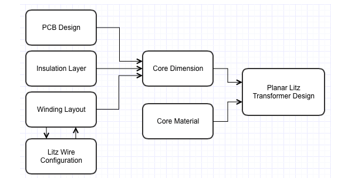
Figure 1. Design procedure of planar transformer
Figure 1 demonstrates the design procedure of planar transformer. Wire configuration depends on winding layout, while its double-sided nature alters conductor arrangement. Core dimension is determined by the design of windings, insulation layers and PCBs. Selection of commonly used materials for core is combined with the core dimension to produce the overall design of planar transformer.
2.2. Winding layout
Current flowing through conductors would cause power dissipation in the form of heat and temperature rise in PCBs. A symmetrical winding structure is used to minimise the effect of thermal expansion. The standard thickness of conductor is selected, which is 70 .
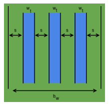
Figure 2. Winding structure
Figure 2 illustrates the fundamental design of winding structure. Based on the international safety standards, the minimum width between two adjacent windings is 150 . The labelled parameters in Figure 2 follow the equation: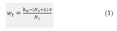
2.3. Strand layout
The length of strand varies as the strand angle changes. The relationship between average length of strands, , width of PCB, , and strand angle, , is given by the following inequality [2]:![]()
The electrical isolation requirements of strands in litz wire configuration is relatively low, because of the minimised potential difference between adjacent strands. Therefore, the space between strands is designed to be small in order to maximise the surface utilisation factor. Reduced gap would, however, make proximity effect significant. Therefore, there is a trade-off between surface utilisation factor and AC resistance in litz wire configuration.
2.4. Insulation layout
Plexiglass is one of the common materials used for insulating conductors. It has widespread utilisation when toughness and thermal conductivity are required.
2.5. PCB design
The standard thickness of a PCB is 1.6 mm, and it is applied in this design. The dimension of PCB is adjusted based on the industrial availability of core, particularly the window size of the core section.
2.6. Core material
The selection of core material is based on three critical characteristics: saturation flux density, permeability and resistivity. High saturation flux density is required to prevent core saturation under high operating frequency. High permeability alleviates the effect of leakage flux and fringing, so that magnetic flux is more concentrated in the core. High resistivity would reduce the power loss caused by eddy current.
There are two commonly used ferromagnetic materials in high frequency transformer, 3F3 and 3F4[3,4]. Both are suitable for medium frequency applications ranging from 10kHz to 2MHz [1]. Moderate permeability and saturation flux density also make them to be optimal in planar transformer.
The optimal operating frequency of two materials are different. 3F3 operates between 10kHz and 500kHz, and the saturation flux density is 370 mT at 100 [2]. 3F4 can operate at 2MHz, and its saturation flux is 350 mT at 100 [4]. Therefore, both materials are used in the design for a wide range of result.
2.7. Design summary
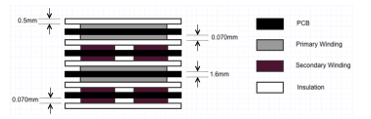
Figure 3. Cross-section of designed planar transformer
Figure 3 shows the cross section of the designed structure. The thicknesses of different layers are labelled based on the design. The total thickness is calculated as:![]()
The core dimension is selected based on the total thickness and the industrial availability, and E43/10/28 is selected. The winding configuration is set to be interleaved for the purpose of minimising the leakage inductance. The overall structure of the planar transformer is shown in Figure 4.
Figure 4. Cross section of overall design
3. Simulation of planar transformer.
3.1. Modelling of planar transformer in Maxwell 3D
The 3D structure of planar transformer is separated into two main parts: windings and core. Figure 5 shows the 3D structure of windings, PCBs and insulation layers. All layers are assigned to different materials based on the theoretical design.
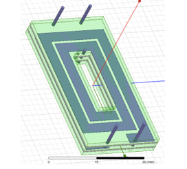
Figure 5. 3D model of windings and PCBs
Figure 6 shows the 3D modelling of core section. Materials are used accordingly to the operating frequency range. Two EE segments are modelled with small air gaps included for simulating real applications.
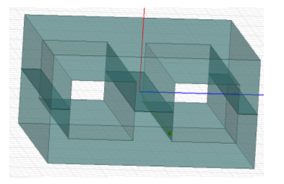
Figure 6. 3D model of core section
Figure 7 shows the overall model of planar transformer, and it is used for field analysis. Current density distribution and electrical parameters under different operating frequencies are evaluated.
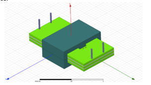
Figure 7. 3D model of planar transformer
3F3 and 3F4 are not standard materials in Maxwell 3D. Assumptions have been made to reduce the time of simulation. Relative permeability is assumed to be constant, and the operating temperature is fixed at 70 degrees for constant conductivity and permeability.
Maxwell 3D applies iteration method to solve mesh equations. The iteration convergence is set to be 5% for accurate result.
3.2. Litz wire 3D modelling
Compared to planar transformer using solid conductor, the liz wire winding structure is also modelled for comparing the overall performance.
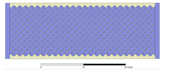
Figure 8. 3D model of litz wire configuration
Figure 8 shows the design of litz wire configuration. This winding structure could provide a relatively uniform current distribution across the conductor, which alleviates the skin effect.
According to the theory, with uniform current distributed across the cross-section of conductors, the AC resistance of litz wire is much smaller than that of transformer using solid conductor. This is, however, not always the case which is proved in the following simulation.
4. Field analysis
4.1. Simulation results
Figure 9 shows the electric field distribution in secondary winding. The copper loss of the winding can be calculated from the electric field strength and the conductivity of copper, and this loss is used as an intermediate result for iterative calculations.
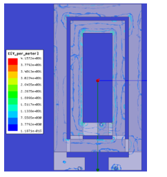
Figure 9. Electric field distribution
Figure 10 shows the fringing effect of air gap. This air gap is placed intentionally to simulate the non-perfect assembly of two EE ferrite segments. Large air gap is avoided for a concentrated magnetic flux density.
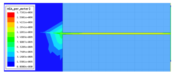
Figure 10. Magnetic field in air gap
Further simulation results, including current density distribution and AC resistance of both solid conductor and litz wire structure, can be found in [5].
4.2. Discussion
The AC resistance of litz wire is relatively smaller than that of solid conductor under medium frequency range. However, the proximity effect becomes significant under very high operating frequency compensating the benefits from the uniform current density distribution.
This proves that the application of litz wire structure is appropriate in a certain frequency range. Operating at frequency outside this range would result in low efficiency, and the solid conductor should be applied instead of litz wire.
5. Design of DC-DC converter
5.1. DC-DC schematic
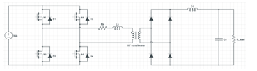
Figure 11. Circuit schematic of PSFB DC-DC converter
Figure 11 shows a PSFB DC-DC converter using a high frequency transformer installed between two DC stages. Possible switching on-states are listed as follow: S1 and S4, S1 and S2, S2 and S3, S3 and S4. The gating signals are shown in Figure 12.
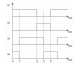
Figure 12. Gating signals
5.2. Derivation of transfer functions
The transfer functions are derived from a unified approach of
modelling switching converter, the state space averaging method, which requires possible state functions of corresponding switching state [6].
Let be the turns ratio, where N1 and N2 are the number of turns on primary and secondary side; V1, V2, i1 and i2 be the voltages and currents of two sides respectively. Assume that electrical parameters follow transformer dot convention.
State 1: . Switches S1 and S4 are turned on, and current at primary side is drawn from voltage source and increases linearly. The circuit is shown in Figure 13.
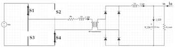
Figure 13. Circuit schematic of state one
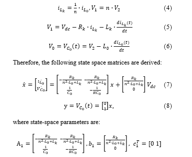
Applying this method to the other three states, with the assumption that and Rk is negligible, the average of state equations is derived for the corresponding time duration.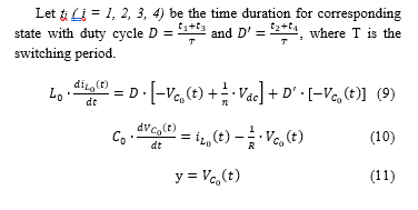
For small signal analysis, time-variant parameters are separated into two parts: static and small signal. Parameters with bar and hat are used to represent small-signal and static parts respectively.
By omitting DC and second-order small terms, small signal equations can be derived: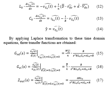
With the assumption that output current and input DC voltage are constant, a AC small-signal model of DC-DC PSFB converter can be obtained using these transfer functions. The system schematic is shown in Figure 14
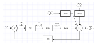
Figure 14. Small-signal model of PSFB DC-DC converter
5.3 Simulation in Simulink
Figure 15. Circuit schematic of PSFB DC-DC converter
Figure 15 shows the circuit schematic of designed PSFB DC-DC converter. Assume that input voltage and output current are constant, the open loop transfer function is simplified into:![]()
The design of feedback loop is shown in Figure 16, including inputs, function blocks and outputs:
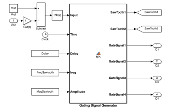
Figure 16. Feedback loop of DC-DC converter
Figure 17 shows the step response of the closed-loop transfer function, which is calculated from the open loop transfer function.
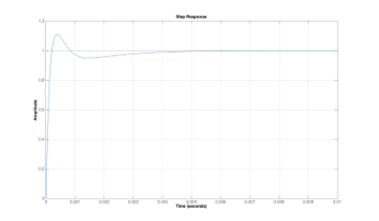
Figure 17. Step response of closed-loop transfer function
Further simulation results, including output voltage waveforms and total harmonic distortion result, are presented in [4]. The design and simulation results of HCC DC-AC inverter can also be found in [4].
5.4. Discussion
With the proper application of state space average method and design of feedback loop, both DC and AC voltages could stabilise at target values with small transient time. The total harmonic distortion of AC voltage is small illustrating a smooth AC waveform.
The phase shift between the converted AC signal and the reference signal from power grid is insignificant and negligible, which proves that this AC output signal can be connected to the power grid.
6. Conclusion
At high frequency range, the operating performance of planar transformer is primarily dependent on the frequency. Litz wire winding configuration is preferred under high frequency range, but its manufacturing complexity and cost need to be considered during the process of design.
In addition, by applying the state space averaging method with reasonable assumptions combined, an accurate open loop transfer function of PSFB DC-DC converter is derived. The DC output voltage of this converter can stabilise at required reference voltage within a short period of time. Additional DC-AC inverter can be easily installed to convert DC power into AC power at target amplitude and frequency for AC applications.
Further study could be done in the electromagnetic field analysis, including current density and magnetic flux density distribution. With more sophisticated devices used, a more comprehensive analysis could be performed and a more reasonable simulation result can be obtained.
Conflict of Interest
The authors declare no conflict of interest.
Acknowledgment
I would like to express my gratitude to the School of Electrical Engineering and Telecommunications UNSW for providing necessary resources to conduct this research.
I would also like to thank my family and friends who have supported and encouraged me throughout the time.
- Z. Ouyang and M.A. Andersen, “Overview of planar magnetic technology – fundamental properties”, IEEE Trans. Power Electronics, vol. 29, No. 9, 2014.
- Shen Wang, Michael Andrew de Rooij, Willem Gerhardus Odendaal, Jacobus Daniel van Wyk, and Dushan Boroyevich, “Reduction of High-Frequency Conduction Losses Using a Planar Litz Structure”, IEEE Transactions on Power Electronics, Vol. 20, No. 2, 2005, pp. 261-267.
- Ferroxcube, “3F3 material specification”. Datasheet, 2004
- Ferroxcube, “3F4 materoal specification”. Datasheet, 2004.
- C. Lian and D. Zhang, “Field-circuit analysis of planar transformer at medium frequency for converter application”, IEEE Annual Southern, Power Electronics (SPEC), 2016.
- R.D. Niddlebrook and S. Cuk, “A general unified approach to modelling switching-converter power stages”, Power Electronics Specialists Conference, pp. 18-34, June 1976.